
- The Growing Demand for Ultra-Fine HDI Flexible Circuits
- Why 50-Micron Lines Fail: The Lithography Challenge
- Laser Microvias: Precision Requirements and Common Pitfalls
- Design Strategies That Enhance Manufacturing Reliability
- Real-World Case Studies: Success and Failure in HDI Flexible PCB Manufacturing
- The Value of Manufacturing Partnership
- Conclusion: Manufacturing Excellence as Competitive Advantage
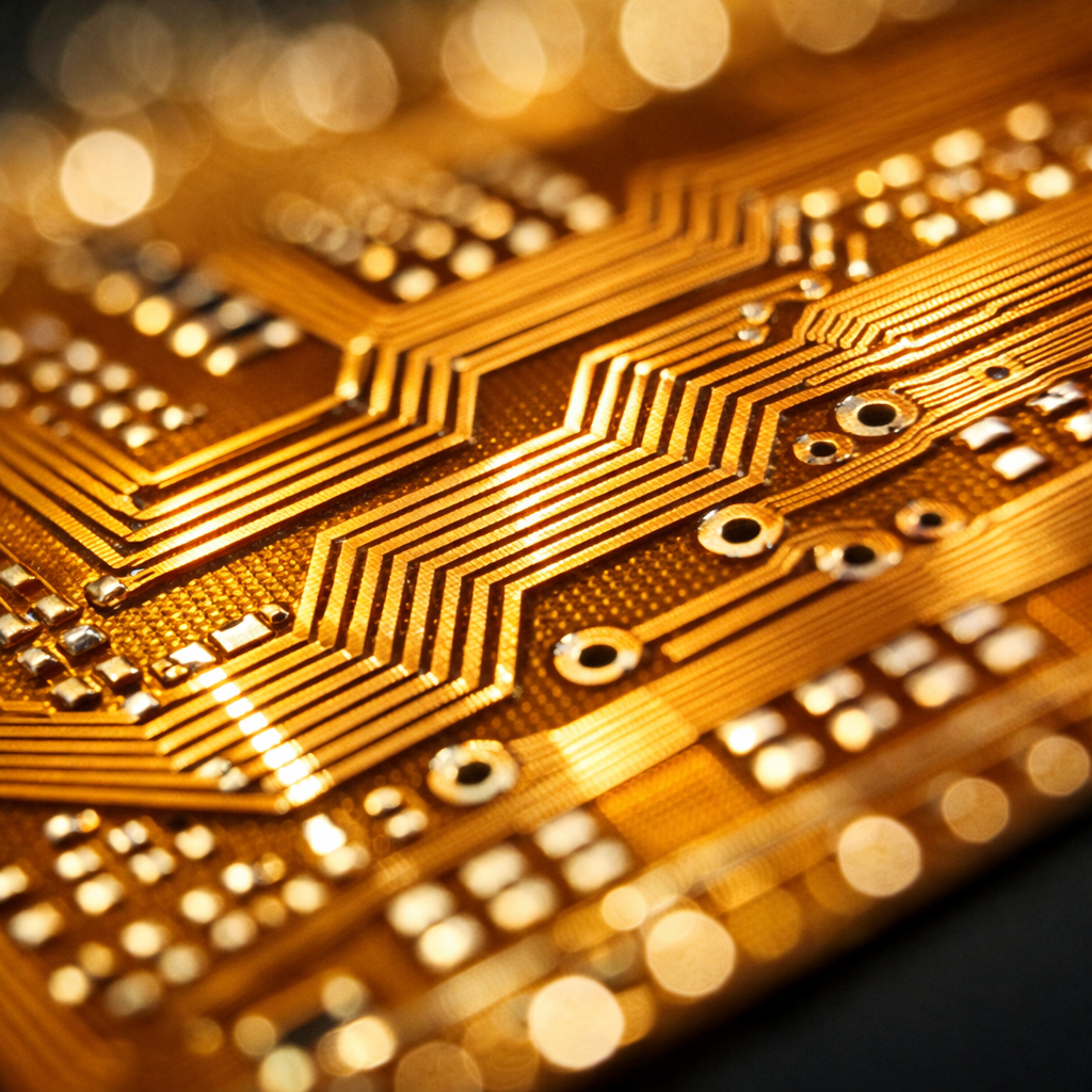
The electronics industry demands ever-smaller form factors without compromising performance. High-density interconnect (HDI) flexible PCBs represent the frontier of miniaturization, enabling compact designs in automotive sensors, medical implants, and aerospace systems. Yet many manufacturers struggle with a persistent challenge: achieving reliable 50-micron lines and functional laser microvias at production scale.
When your prototype works perfectly but production units fail thermal cycling tests, the problem often lies not in design intent but in manufacturing execution. Understanding why these fine features fail—and how to prevent those failures—separates successful product launches from costly delays.
The Growing Demand for Ultra-Fine HDI Flexible Circuits
Modern electronic devices pack extraordinary functionality into shrinking spaces. An electric vehicle battery management system might integrate dozens of temperature sensors on a single flexible circuit measuring just millimeters wide. Medical wearables monitor vital signs through flexible sensors that conform to body contours. These applications demand HDI flexible PCBs with line widths approaching 50 microns and microvia diameters under 100 microns.
The automotive sector exemplifies this trend. IATF 16949-certified flexible circuits in EV applications must handle high current densities while fitting within tight chassis constraints. A typical automotive camera module might require 200 signal traces in a 15mm width—achievable only through HDI techniques combining ultra-fine lines with stacked microvias.
Medical device manufacturers face similar pressures. ISO 13485-compliant flexible circuits for minimally invasive surgical tools demand extreme miniaturization while maintaining absolute reliability. A single interconnect failure in a catheter guidance system could have serious consequences during a procedure.
These applications share a common requirement: consistent quality at production volumes. A prototype that performs flawlessly means nothing if manufacturing yields drop below 95% during mass production.
Why 50-Micron Lines Fail: The Lithography Challenge
Achieving 50-micron trace widths on flexible substrates requires precision lithography, controlled etching, and uniform copper deposition. Each step introduces potential failure modes that manifest differently than in conventional PCB manufacturing.
The first challenge emerges during photoresist application. Flexible polyimide substrates don’t lie perfectly flat like rigid FR-4 boards. Even slight warping creates focal plane variations during exposure, causing some traces to receive insufficient UV energy while others get overexposed. The result: inconsistent trace widths that measure 48 microns in one area and 53 microns in another.
Temperature control during exposure proves critical. A lithography process calibrated at 22°C produces different results at 24°C because photoresist sensitivity changes with temperature. This variability explains why production runs succeed in climate-controlled facilities but fail when ambient conditions fluctuate.
Etching presents the second major challenge. The chemical etching process removes unwanted copper, but etchant penetrates beneath photoresist edges through a phenomenon called undercutting. For 50-micron lines, even 3-4 microns of undercutting can reduce trace width by 12-16%. Worse, undercutting varies with etchant concentration, temperature, and agitation—factors difficult to maintain consistently across eight-hour shifts.
Consider a production scenario: Morning batches with fresh etchant produce clean 50-micron lines, but by afternoon, depleted chemistry causes excessive undercutting, reducing widths to 44 microns. The electrical resistance increases, thermal performance degrades, and finished circuits fail accelerated life testing.
Copper deposition uniformity creates the third failure mode. Electroplating deposits copper through ionic transfer, but current density varies across panel surfaces. Panel edges receive higher current density than centers, resulting in thicker copper at peripheries. For ultra-fine traces, this thickness variation creates impedance mismatches that disrupt high-speed signals.
A telecommunications equipment manufacturer discovered this issue when optical transceiver modules failed at production scale. Laboratory prototypes performed perfectly, but production units showed signal integrity problems. Investigation revealed 3-micron copper thickness variations along 50-micron traces—enough to create impedance shifts that degraded 10Gbps signals.
Laser Microvias: Precision Requirements and Common Pitfalls
Laser-drilled microvias enable vertical interconnections between flexible PCB layers without consuming valuable routing space. These tiny holes—typically 75-100 microns in diameter—allow HDI designs to achieve routing densities impossible with mechanical drilling. Yet microvias introduce unique failure modes that catch many manufacturers unprepared.
The laser drilling process ablates dielectric material using focused UV or CO₂ laser pulses. Success depends on precise energy control: too little energy leaves residual resin (smear) that prevents proper copper plating, while excessive energy damages the underlying copper pad or creates rough sidewalls.
Material characteristics significantly impact drilling outcomes. Standard polyimide substrates absorb laser energy predictably, but adhesive layers between copper and polyimide respond differently. When laser energy reaches the adhesive, it can cause micro-delamination around the via—invisible initially but catastrophic during thermal cycling.
One aerospace contractor experienced this failure mode in attitude control sensors for satellite applications. Qualification testing revealed that 8% of microvias failed after 500 thermal cycles between -40°C and +125°C. Failure analysis showed adhesive delamination initiated during laser drilling, then propagated during thermal stress. The solution required switching to adhesiveless polyimide substrates and optimizing laser parameters—changes that delayed program launch by four months.
Microvia plating creates additional challenges. Copper must deposit uniformly along via sidewalls to ensure electrical continuity and mechanical strength. Poor plating leaves voids—particularly at the via “knee” where sidewall meets pad. These voids create stress concentration points that crack during flexing or thermal cycling.
The manufacturing challenge intensifies with stacked microvias, where holes in successive layers align vertically. Each via requires precise drilling registration and uniform plating. Misalignment by just 15 microns between layer pairs causes the via stack to miss the target pad, creating intermittent connections that fail unpredictably during use.
An automotive tier-one supplier encountered this issue in electric power steering modules. Field returns showed electrical failures after 50,000-100,000 steering wheel rotations. Root cause analysis identified misaligned stacked microvias that created high-resistance joints. Under repeated flexing, these joints heated up, accelerating copper oxidation until complete failure occurred.
Design Strategies That Enhance Manufacturing Reliability
Successful HDI flexible PCB manufacturing requires designs optimized for production realities. Engineers can incorporate several strategies that dramatically improve yield without compromising functionality.
Via-in-pad placement offers significant advantages for HDI designs. Rather than routing traces away from component pads to reach vias, placing microvias directly within pads shortens signal paths and reduces routing congestion. However, this approach requires careful resin flow management during lamination. Insufficient resin flow leaves voids beneath components, while excessive flow causes pad non-planarity that prevents proper solder joint formation.
A medical device manufacturer resolved this challenge using proprietary resin flow modeling developed with manufacturing partners. By simulating resin behavior during lamination cycles, engineers optimized via fill requirements before committing to production tooling. The result: first-pass yield improved from 87% to 96% for a glucose monitoring sensor incorporating 240 via-in-pad connections per unit.
Stack-up symmetry proves crucial for flexible PCB reliability. Asymmetric copper distribution creates differential thermal expansion that causes warping during reflow soldering. For a six-layer HDI design, placing copper layers symmetrically around the center plane ensures balanced expansion forces. This seemingly simple principle prevents issues that manifest as component placement shifts or tombstoning during assembly.
Trace width variation management requires understanding manufacturing capabilities. Specifying 50-micron traces uniformly across a design ignores the reality that manufacturing tolerances vary with location. Better approaches assign 50-micron widths only where absolutely necessary for routing density, using 75-100 micron traces elsewhere. This targeted approach improves manufacturability while meeting design requirements.
Tearaway tabs and routing channels offer another practical solution. These sacrificial features along panel edges allow test coupons for process monitoring without consuming valuable circuit area. When production issues arise, test coupons reveal whether problems stem from lithography, etching, or plating—enabling rapid corrective action before entire batches are scrapped.
A consumer electronics manufacturer implemented this approach for smartphone camera modules containing 180 HDI traces per square centimeter. Test coupons positioned every 50mm across production panels provided real-time process feedback. When morning shift coupons showed 2-micron trace width drift, technicians immediately adjusted etching parameters, preventing defects from reaching production circuits.
Real-World Case Studies: Success and Failure in HDI Flexible PCB Manufacturing
A European automotive supplier developing next-generation ADAS sensors faced repeated failures during environmental testing. The flexible PCB design incorporated 50-micron traces and 80-micron microvias in a four-layer stack-up. Laboratory prototypes passed all requirements, but production units failed thermal shock testing at -40°C to +125°C.
Investigation revealed three interconnected issues. First, microvia plating showed 12-15% void formation—acceptable for low-stress applications but inadequate for automotive thermal cycling. Second, adhesive layers between copper and polyimide contributed to z-axis thermal expansion mismatches. Third, trace width variations of 4-6 microns created localized current density increases that accelerated electromigration.
The solution required a comprehensive approach. Switching to adhesiveless polyimide substrates eliminated z-axis expansion problems. Optimizing laser drilling parameters reduced via voiding to under 3%. Tightening lithography process controls reduced trace width variation to ±2 microns. The combined improvements elevated thermal cycling performance from 280 cycles (average) to over 1,000 cycles—exceeding automotive qualification requirements.
Contrast this with a medical device manufacturer developing implantable cardiac monitors. Their HDI flexible design used 60-micron traces rather than pushing to 50 microns, accepting slightly larger form factor for improved manufacturability. Microvias employed staggered rather than stacked configurations, reducing drilling precision requirements. The result: first-pass production yield of 94% and zero field failures in 18 months of commercial production.
An industrial automation company learned similar lessons developing flexible circuits for robotic arm joint sensors. Initial designs specified 45-micron traces to minimize sensor profile. Production yields struggled at 78%, with failures concentrated in high-flex zones. Redesigning with 65-micron traces in flex regions—while maintaining 45-micron traces in rigid mounting areas—improved yield to 93% while meeting size requirements.
These cases illustrate a common theme: successful HDI flexible PCB manufacturing balances design ambition with production reality. Engineers who collaborate closely with manufacturing partners identify optimal approaches that achieve functional requirements reliably at scale.
The Value of Manufacturing Partnership
Achieving reliable HDI flexible PCB production requires more than advanced equipment—it demands manufacturing expertise developed through years of production experience. This explains why companies like Flex Plus (Xiamen) Co., Ltd emphasize complete manufacturing control rather than relying on broker networks.
With 20+ years specializing in flexible PCB manufacturing, Flex Plus has developed proprietary methodologies for ultra-fine feature production. Their capabilities extend to 0.05mm line width and spacing (2mil/2mil)—industry-leading specifications backed by ISO 9001, ISO 13485, and IATF 16949 certifications.
The difference emerges during design consultation. Rather than simply accepting customer designs, experienced manufacturers provide comprehensive Design for Manufacturability (DFM) analysis. Engineers identify potential yield limiters early—before costly tooling commits designs to production. This collaborative approach reduces prototype iterations from an industry average of 3.2 cycles to 1.8 cycles, accelerating time-to-market by months.
Manufacturing control matters especially for HDI production. When a single organization controls every process step—from raw polyimide through final electrical testing—process optimization becomes systematic rather than fragmented. Changes in laser drilling parameters can be coordinated with plating adjustments, creating synergistic improvements impossible when processes are distributed across multiple vendors.
Consider thermal management requirements for high-power LED applications. Flex Plus’s pioneering flexible heat dissipation technology integrates thermal pathways directly into HDI stack-ups, addressing thermal challenges at the manufacturing level rather than requiring secondary heat sink attachments. This innovation emerged from complete manufacturing control that enabled cross-functional collaboration between materials engineering, process development, and design teams.
Conclusion: Manufacturing Excellence as Competitive Advantage
As electronic devices continue shrinking while functionality expands, HDI flexible PCBs with ultra-fine features become essential rather than optional. Success requires understanding not just circuit design principles but manufacturing realities that determine production outcomes.
When your 50-micron lines and laser microvias keep failing, the solution lies in manufacturing partnership with organizations possessing proven capabilities, comprehensive certifications, and two decades of specialized experience. Companies that view manufacturers as engineering partners—rather than commodity suppliers—gain access to proprietary processes, DFM insights, and rapid problem resolution that transform challenging designs into production successes.
The electronics industry rewards those who recognize that innovation requires not just creative design but manufacturing excellence. For organizations seeking reliable HDI flexible PCB solutions from prototypes through mass production, partnering with specialized manufacturers offering complete manufacturing control and certified quality systems provides the foundation for competitive advantage in markets where product reliability defines brand reputation.