
- Understanding the Unique Heat Challenges in Flex PCBs
- Core Design Principles for Thermal Management
- Thermal Via Strategies: Creating Vertical Heat Highways
- Heat Spreading and External Heat Sink Options
- Material and Adhesive Selection for Thermal Performance
- Practical Layout and Assembly Considerations
- Testing, Validation, and Verification Methods
- Design Checklist: Key Thermal Management Considerations
When your flexible PCB prototype works perfectly at low power but fails thermal testing at production loads, you’re facing one of the most common—and frustrating—challenges in high-power flex circuit design. Unlike rigid PCBs with their thick FR-4 substrates and generous copper layers, flexible circuits present unique thermal management obstacles that can turn an elegant design into an overheating nightmare.
The problem isn’t always obvious during initial testing. A flex PCB might handle brief power bursts without issue, only to develop hot spots during sustained operation. Components start drifting out of specification. Solder joints weaken. In extreme cases, the polyimide substrate itself begins degrading. These failures often emerge late in development—sometimes not until field deployment—when fixes are expensive and time-consuming.
At Flex Plus, we’ve spent over 20 years helping engineers navigate these thermal challenges across industries from automotive power electronics to medical device implants. The solutions aren’t always intuitive, but they follow clear engineering principles. Let’s explore why your high-power flex design keeps overheating and what you can do about it.
Understanding the Unique Heat Challenges in Flex PCBs
Flexible PCBs face thermal constraints that rigid boards simply don’t encounter. The very properties that make them flexible—thin substrates, minimal copper weight, bendable construction—work against efficient heat dissipation.
Consider a typical double-sided flex circuit: you’re working with 25 to 50 microns of polyimide, 18 to 35 microns of copper on each side, and perhaps another 25 microns of coverlay. The entire stackup might be thinner than a human hair. Compare this to a rigid PCB with 1.6mm FR-4, multiple copper planes, and substantial thermal mass. The flex circuit has nowhere to store heat and limited pathways to move it away.
Localized hot spots become the primary concern. A power component generating 2 watts on a rigid board might see a modest temperature rise. That same component on a flex circuit can create a hot spot exceeding 150°C because heat cannot spread laterally through thin copper traces or dissipate through a minimal substrate. The problem compounds when multiple components cluster together—common in space-constrained designs where flex circuits typically excel.
The bendable nature of flex circuits introduces another variable: thermal performance changes with mechanical state. A flex circuit lying flat may achieve acceptable thermal performance, but the same circuit bent at 90 degrees concentrates heat differently. Trace resistance increases slightly with each bend radius, generating additional I²R heating. If your design requires dynamic flexing during operation, thermal hotspots can migrate as the circuit moves.
Material limitations further constrain your options. Polyimide offers excellent electrical properties and flexibility, but its thermal conductivity (around 0.1-0.2 W/m·K) pales compared to FR-4 (0.3 W/m·K) or aluminum substrates (200+ W/m·K). You cannot simply specify thicker copper without compromising flexibility. A flex circuit with 70-micron copper becomes noticeably stiffer and more prone to fatigue cracking at bend points.
These challenges don’t make flex PCBs unsuitable for high-power applications—they simply require thoughtful thermal management strategies from the earliest design stages.
Core Design Principles for Thermal Management
Effective thermal management in flexible PCBs starts with fundamental design principles that work within the constraints of thin, bendable substrates. The goal isn’t to match rigid PCB thermal performance but to create adequate heat pathways given the available materials and geometry.
Component distribution forms your first line of defense. Spreading high-power components across the available board area prevents heat concentration. If your design places a power regulator, LED driver, and radio module within a 10mm radius, you’re creating a thermal disaster regardless of other mitigation strategies. Physical separation allows each component to dissipate heat through its local copper area without competing with neighboring heat sources.
When physical separation isn’t possible—and in compact designs it often isn’t—strategic component placement becomes critical. Position high-power components near board edges or areas that will remain flat during use. Avoid placing them at tight bend radii where heat dissipation is already compromised. In rigid-flex designs, locate power components on rigid sections where you can implement more aggressive cooling strategies.
Copper pours and ground planes serve double duty in flex circuits: electrical distribution and heat spreading. A continuous copper pour under a hot component acts as a heat spreader, distributing thermal energy over a larger area. The thinner your substrate, the more important this becomes. Even with 18-micron copper (½ oz), a properly sized pour significantly reduces peak temperatures compared to isolated component pads.
The stackup itself offers thermal optimization opportunities. While flex circuits rarely exceed four layers for cost and flexibility reasons, even a four-layer design allows strategic placement of copper planes. Position your ground plane directly under high-power components. The continuous copper sheet provides a lower-resistance thermal path than individual traces. In multilayer rigid-flex designs, consider dedicating inner layers to thermal management rather than signal routing where thermal demands justify it.
Stiffeners play an underappreciated role in thermal management. While primarily added for mechanical support or connector reinforcement, a stiffener creates a thermal mass that absorbs transient heat and provides a mounting surface for external heatsinks. FR-4 or polyimide stiffeners with copper backing offer better thermal performance than simple polyimide reinforcement. At Flex Plus, we’ve seen well-placed stiffeners reduce component temperatures by 15-20°C in high-power LED applications.
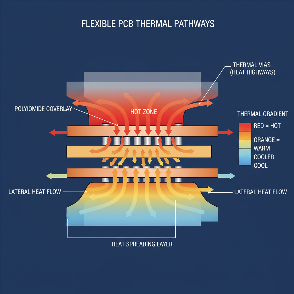
Thermal Via Strategies: Creating Vertical Heat Highways
Thermal vias represent one of the most effective tools for managing heat in flexible PCBs, yet they’re often underutilized or incorrectly implemented in flex circuit designs. These small copper-plated holes create vertical thermal highways that move heat from surface-mounted components to internal copper layers or the opposite side of the board.
The principle is straightforward: copper conducts heat roughly 400 times better than polyimide. A 0.3mm diameter thermal via, properly plated with 25 microns of copper, creates a direct thermal connection through your substrate. An array of these vias under a hot component acts like a heat pipe, transferring thermal energy away from the source.
Effective thermal via implementation requires attention to several parameters. Via diameter, plating thickness, and spacing all impact thermal performance. Larger vias conduct more heat but compromise flexibility more severely. Smaller vias (0.2-0.3mm) maintain flexibility better but require more vias to achieve equivalent thermal transfer. The copper plating thickness matters enormously—thin plating creates a bottleneck that limits heat transfer. We recommend minimum 25-micron plating thickness for thermal vias, preferably 35 microns for high-power applications.
Via placement follows specific patterns for optimal thermal performance. Place thermal vias directly under component thermal pads, creating the shortest possible thermal path. For packages with exposed thermal pads or ground slugs, a via array filling the pad area maximizes heat transfer. Typical spacing runs 0.8-1.5mm between vias, balancing thermal performance against manufacturing complexity and flexibility impact.
The connection point matters as much as the vias themselves. Thermal vias should terminate at substantial copper areas—ground planes, large copper pours, or external thermal pads. A via that terminates at a narrow trace accomplishes little. The receiving copper area acts as a heat spreader, distributing the transferred thermal energy across a larger surface area for dissipation.
- Filled or capped vias offer enhanced performance but at additional cost. Standard through-hole vias can trap air that limits thermal conductivity. Learn more about thermal via design trade-offs in flexible circuits. Filling vias with conductive epoxy eliminates air gaps and adds thermal mass. Capping vias with copper during plating creates a sealed thermal pathway. These processes add cost but provide measurable temperature reductions in demanding applications. For automotive or medical device applications where reliability justifies additional investment, filled thermal vias often make sense.
Heat Spreading and External Heat Sink Options
Beyond via-based thermal pathways, flexible PCB designs benefit from deliberate heat spreading strategies and, where appropriate, external heat management solutions. The challenge lies in implementing these strategies without sacrificing the flexibility and compact form factor that drove your choice of flex circuits in the first place.
Extended copper pours represent the simplest heat spreading approach. Rather than limiting copper to required traces and pads, extend copper fills across available board area. These copper regions act as heat spreaders, distributing thermal energy over larger surfaces where it can dissipate through radiation and convection. Even thin 18-micron copper provides significant heat spreading when properly sized. The trade-off involves reduced flexibility and increased copper etching requirements, but for static or infrequently flexing sections, extensive copper pours make excellent sense.
Embedded heatsinks integrate directly with flex circuit assemblies for applications demanding more aggressive thermal management. A thin aluminum or copper plate bonded to the flex circuit acts as a heat spreader and heatsink. This approach works particularly well in rigid-flex designs where the heatsink attaches to rigid sections. Automotive LED lighting assemblies often use this technique, bonding flex circuits to aluminum backing plates that serve as both mechanical support and thermal management. The bonding adhesive becomes critical—poor thermal interface resistance between flex circuit and heatsink undermines the entire approach.
Thermally conductive adhesives and gap fillers create thermal pathways between flex circuits and external structures. These materials bridge air gaps that would otherwise insulate the circuit. Selecting appropriate materials requires balancing thermal conductivity (measured in W/m·K), flexibility, and bonding strength. Materials range from basic thermal tapes (1-2 W/m·K) to advanced phase-change materials (4-6 W/m·K) that flow under heat to eliminate microscopic gaps. For flex circuits that require dynamic bending, the adhesive must flex without delaminating or compromising thermal performance.
External heatsink attachment in flex circuits requires creative mechanical solutions. Traditional heatsink clips and fasteners work poorly with thin, flexible substrates. Successful approaches include bonding heatsinks to stiffened areas, integrating heatsink attachment points into rigid sections of rigid-flex boards, or using compliant thermal interface materials that accommodate flex circuit movement. We’ve developed specialized attachment methods for clients in telecommunications, where optical transceiver modules require substantial heat management while maintaining the cable-like routing flexibility of flex circuits.
Graphite thermal pads offer an emerging solution for flex circuit thermal management. These thin, highly conductive sheets (thermal conductivity 400+ W/m·K in-plane) can be laminated to flex circuits, providing exceptional lateral heat spreading without significantly compromising flexibility. They work particularly well for distributing heat from point sources across larger areas. The technology is still evolving for flex circuit applications, but early implementations in smartphones and wearables show promise.
Material and Adhesive Selection for Thermal Performance
The materials that comprise your flexible PCB stackup fundamentally determine thermal performance limits. While designers naturally focus on electrical properties, thermal characteristics of base materials, copper weights, and adhesives dramatically impact heat management capability.
Polyimide remains the standard flex circuit substrate material, offering excellent electrical properties, chemical resistance, and flexibility. However, standard polyimide’s thermal conductivity (0.1-0.2 W/m·K) represents a significant thermal barrier. For applications requiring enhanced thermal performance, consider alternative substrate materials and their thermal characteristics. Specialty polyimides with enhanced thermal conductivity are available, achieving 0.3-0.5 W/m·K through ceramic or metallic fillers. These materials cost more but provide measurable temperature reductions in high-power applications. The trade-off involves slightly reduced flexibility and more complex processing requirements.
Adhesive selection deserves particular attention because adhesives often create the largest thermal resistance in flex circuit stackups. Traditional acrylic adhesives used in many coverlay films have poor thermal conductivity (0.2-0.3 W/m·K). Worse, adhesive layers add thickness without adding thermal pathways. Adhesiveless constructions, where coverlay bonds directly to copper through cast coating, eliminate this thermal resistance layer entirely. At Flex Plus, we recommend adhesiveless constructions for high-power applications whenever mechanical requirements permit.
Copper weight selection balances electrical and thermal performance against flexibility. Thicker copper (35 or 70 microns) provides better current carrying capacity and heat spreading but reduces flexibility and increases minimum bend radius. For circuits requiring dynamic flexing, 18-micron copper often represents the optimal compromise. Static sections or rigid areas of rigid-flex boards can employ heavier copper where thermal management demands it. Strategic use of varying copper weights across the same board—thick copper in static high-power zones, thin copper in flex areas—optimizes both thermal and mechanical performance.
Coverlay materials contribute to overall thermal performance, though their impact is often overlooked. Standard polyimide coverlay with acrylic adhesive adds thermal resistance without adding heat capacity. Thinner coverlays (25 microns vs. 50 microns) reduce thermal resistance while still providing adequate insulation. For extreme applications, photoimageable coverlay coatings eliminate adhesive entirely and can be applied as thin as 15 microns, minimizing thermal barriers.
Material compatibility under thermal stress requires verification beyond room-temperature specifications. Adhesives that bond perfectly at 25°C may delaminate at 120°C operating temperatures. Thermal cycling from -40°C to +125°C—common in automotive applications—stresses material interfaces through differential expansion. At Flex Plus, our IATF 16949 certification requires rigorous thermal cycling qualification to verify material compatibility under real-world thermal conditions. This testing has prevented countless field failures in automotive electronics where thermal management is critical.
Practical Layout and Assembly Considerations
Theory translates to practice through careful layout and assembly execution. Even the best thermal management strategy fails if implementation overlooks practical manufacturing and assembly realities.
Trace routing impacts thermal performance more than many designers realize. Wide traces carry more current with less resistance heating. For power distribution in flex circuits, minimize trace length and maximize trace width within layout constraints. A 0.5mm trace carrying 2A generates significantly more heat than a 1mm trace carrying the same current. Calculate I²R losses for every power trace and size accordingly. In high-power sections, consider using copper pours instead of traces altogether—treat power distribution like a plane rather than individual connections.
Component pad design affects both thermal and electrical performance. Larger pads provide better heat sinking for components but increase soldering challenges in thin flex substrates. Thermal relief pads help during assembly by preventing excessive heat transfer into copper planes during soldering, but they also create thermal resistance during operation. For high-power components, full thermal connection often outweighs assembly convenience. We work closely with clients to balance manufacturability against thermal requirements.
Assembly process considerations become critical with thermally challenging designs. Flex circuits have less thermal mass than rigid boards, making them more susceptible to heat damage during assembly. Reflow profiles require careful optimization to prevent substrate damage while achieving reliable solder joints. Wave soldering often proves difficult with flex circuits due to substrate flexibility and warping under heat. At Flex Plus, our comprehensive PCBA services include optimized assembly processes specifically developed for flex circuits, ensuring reliable assembly without thermal damage.
Alignment between thermal design and mechanical requirements prevents conflicts. Thermal management often benefits from rigid sections with heatsinks and substantial copper pours. Mechanical design may require flexibility in those exact locations. Early collaboration between thermal, electrical, and mechanical teams identifies these conflicts while design changes remain inexpensive. Rigid-flex technology often provides the ideal solution, placing high-power components and thermal management structures on rigid sections while maintaining flexible interconnections where needed.
Testing and validation close the loop between design intent and manufactured reality. Thermal imaging during powered testing reveals actual hot spots and temperature gradients. We’ve seen countless designs where assumed thermal pathways didn’t perform as expected—vias placed slightly off-center from thermal pads, copper pours inadvertently isolated from ground planes by narrow clearances, or coverlay creating unintended thermal barriers. Early thermal validation catches these issues before tooling commitment.
Testing, Validation, and Verification Methods
No thermal management strategy is complete without rigorous testing and validation. Design calculations and simulations provide excellent guidance, but physical measurement reveals the truth about thermal performance.
Thermal simulation tools offer valuable prediction capability during design. Modern PCB design software includes thermal analysis features that estimate temperature distributions based on component power dissipation, copper geometry, and material properties. These simulations help identify potential hot spots before manufacturing prototypes. However, simulations rely on accurate material properties and boundary conditions. Conservative assumptions about convection, radiation, and thermal interface resistances prevent over-optimistic predictions.
Prototype thermal testing validates design assumptions with real hardware. Thermal imaging cameras provide instant visualization of temperature distributions across your flex circuit. These images immediately reveal hot spots, thermal gradients, and areas where heat isn’t spreading as expected. Temperature measurements should occur under realistic operating conditions—proper airflow, mounted configuration, and full electrical load. A flex circuit cooled by a lab fan may show acceptable temperatures while the same circuit in a sealed enclosure overheats.
Thermocouple placement requires strategic thinking. Surface-mount thermocouples measure component case temperatures, but junction temperatures—where semiconductor failure actually occurs—run higher. Understanding thermal resistance from junction to case (specified in component datasheets) allows calculation of actual junction temperatures. Multiple measurement points across the circuit reveal thermal gradients and validate heat spreading effectiveness.
Environmental testing under temperature extremes verifies robustness. Many applications require operation from -40°C to +85°C or higher. Component power dissipation remains constant, but environmental temperature affects available thermal headroom. A design operating at 80°C junction temperature in 25°C ambient may exceed maximum junction temperature when ambient reaches 65°C. Thermal testing across the full operating temperature range prevents field failures.
Long-term reliability testing reveals degradation over time. Initial thermal performance may prove acceptable, but thermal cycling gradually degrades solder joints, adhesive bonds, and material properties. Accelerated life testing—hundreds or thousands of thermal cycles between temperature extremes—identifies reliability issues before field deployment. This testing is particularly critical for automotive and medical applications where reliability requirements exceed consumer electronics standards.
Design Checklist: Key Thermal Management Considerations
Successful flexible PCB thermal management requires attention to multiple factors throughout the design process. This checklist summarizes critical considerations:
Early Design Phase:
- Calculate worst-case power dissipation for each component
- Identify maximum allowable temperature rise for critical components
- Assess available board area for heat spreading
- Determine mechanical constraints (bend radius, dynamic flexing requirements)
- Select appropriate substrate materials with adequate thermal properties
Layout Phase:
- Distribute high-power components across available board area
- Position power components away from tight bend radii
- Implement copper pours under high-power components
- Design thermal via arrays under thermal pads (minimum 25μm plating)
- Maximize trace widths for power distribution
- Create continuous thermal pathways to heat spreaders or external structures
Stackup Design:
- Position ground planes under high-power components
- Consider adhesiveless constructions for reduced thermal resistance
- Specify appropriate copper weights (heavier in static sections)
- Add stiffeners in high-power regions for thermal mass and heatsink mounting
- Select coverlays with minimal thermal resistance
Manufacturing Considerations:
- Verify thermal via placement aligns precisely with thermal pads
- Ensure adequate copper pour connectivity to ground planes
- Specify appropriate assembly processes for thermally sensitive designs
- Plan for thermal imaging inspection during production testing
Validation Phase:
- Perform thermal simulation to predict hot spots
- Conduct thermal imaging on prototypes under full load
- Measure junction temperatures of critical components
- Test across full operating temperature range (-40°C to +85°C typically)
- Execute thermal cycling qualification (minimum 100 cycles, preferably 500+)
This systematic approach to flexible PCB thermal management transforms a common source of field failures into a controlled, predictable aspect of your design. The investment in proper thermal design early in development prevents expensive redesigns, delayed product launches, and field reliability issues.
At Flex Plus, our 20+ years specializing in flexible and rigid-flex PCB manufacturing means we’ve encountered virtually every thermal management challenge across industries from automotive to medical devices. Our engineering team provides comprehensive design support from initial concept through mass production, helping you optimize thermal performance while maintaining the flexibility, reliability, and manufacturability your application demands. Whether you’re designing electric vehicle battery management systems, medical implant electronics, or high-power LED lighting, effective thermal management separates successful products from expensive failures. The principles outlined here provide the foundation for success—but every application brings unique challenges requiring specialized expertise and proven manufacturing capabilities.