
- The Bend Radius Challenge: Where Most Failures Begin
- Strategic Stiffener Placement: The Unsung Reliability Hero
- Coverlay Protection: Your First Defense Against Environmental Degradation
- Trace Routing Strategies That Minimize Stress Concentration
- Component and Solder Joint Placement: Avoiding Mechanical Failure Points
- Environmental Sealing: Preventing Moisture-Driven Delamination
- Stack-Up Design and Material Compatibility: The Foundation of Reliability
- Via Design in Flex Zones: Managing Mechanical Stress at Interconnections
- Design-for-Manufacturing Reviews and Testing Protocols: Catching Issues Early
- Applying These Insights: Your Path Forward
When a medical device fails in the field or an automotive sensor stops working after a few months, the root cause often traces back to the earliest stages of development—the flexible PCB design itself. Industry data reveals a sobering truth: 87% of early field failures in flexible circuits stem from preventable design mistakes made before manufacturing even begins. For engineers and procurement teams investing significant resources into high-volume production, understanding these pitfalls isn’t just helpful—it’s essential for product reliability and your company’s reputation.
Flexible PCBs power some of the most innovative technologies today, from electric vehicle battery management systems to implantable medical devices. Yet despite two decades of established design guidelines, the same fundamental mistakes continue to compromise circuit reliability across industries. These errors don’t just cause immediate failures—they create subtle weaknesses that manifest months after deployment, when warranty costs and brand damage far exceed the original savings from rushed design decisions.
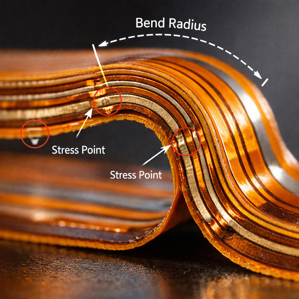
The Bend Radius Challenge: Where Most Failures Begin
The single most common mistake in flexible PCB design involves ignoring established bend radius guidelines. When engineers specify bend radii that are too tight, they initiate a cascade of mechanical stress that eventually leads to copper fatigue and circuit failure. This isn’t theoretical—it’s the primary failure mechanism in dynamic applications where flex circuits move repeatedly.
The mathematics are straightforward but frequently overlooked. For single-layer dynamic PCBs, the minimum bend radius must be at least 100 times the board thickness. If your circuit measures 0.2mm thick, you need a 20mm bend radius minimum. For static applications, you can reduce this to 10-20 times the thickness, but cutting corners here creates reliability risks that emerge during thermal cycling or vibration testing.
Multi-layer designs demand even more generous radii. A three-layer flex circuit requires a minimum bend radius of 12 times its total thickness, while two-layer designs need at least 10 times. These aren’t arbitrary numbers—they’re derived from years of field data showing where copper begins experiencing permanent deformation. When you compress these ratios to save space, you’re essentially programming a future failure into your product.
At FlexPlus, our design-for-manufacturing reviews catch these radius violations before they reach production. With 20+ years of specialized experience across automotive, medical, and aerospace applications, we’ve documented exactly how different stack-ups respond to various bending stresses. This knowledge base allows us to recommend optimal bend radii for each application’s specific duty cycle and environmental conditions.
Strategic Stiffener Placement: The Unsung Reliability Hero
Stiffeners often receive minimal attention during initial design phases, yet their proper application dramatically impacts long-term reliability. These reinforcement elements prevent material fatigue at stress concentration points and maintain alignment during assembly operations. Without them, flexible circuits gradually develop micro-cracks at transition zones between rigid and flex sections.
The critical mistake here involves either omitting stiffeners entirely or placing them incorrectly. Stress-prone areas—particularly where connectors attach or where repeated bending occurs—absolutely require stiffener backing. The material choice matters too: FR-4 stiffeners work well for most applications, but stainless steel provides superior support for high-stress environments like automotive under-hood installations.
Position stiffeners strategically under solder pads and component mounting areas. This reinforcement prevents the peeling forces that occur during thermal expansion and contraction cycles. For circuits experiencing dynamic flexing, extend stiffeners slightly beyond the flex-to-rigid transition zone to distribute stress more evenly. This seemingly minor detail can double the fatigue life of your circuit in field conditions.
Coverlay Protection: Your First Defense Against Environmental Degradation
Inadequate coverlay protection represents another frequent design oversight with serious consequences. The coverlay serves as both electrical insulation and environmental barrier, protecting copper traces from moisture ingress, chemical exposure, and mechanical abrasion. When designers specify insufficient coverlay coverage or choose inappropriate materials, they create pathways for accelerated degradation.
Moisture ingress particularly threatens flexible circuits in automotive and outdoor applications. Water penetrating through inadequate coverlay causes copper oxidation, delamination between layers, and eventually complete electrical failure. The damage often begins subtly—slightly higher resistance measurements that gradually worsen over weeks or months until the circuit stops functioning entirely.
Material selection for coverlay demands careful consideration of operating environments. Polyimide-based coverlay with acrylic adhesive handles most general applications effectively, but high-temperature environments require specialized materials with superior thermal stability. For medical devices requiring biocompatibility, select coverlay materials meeting ISO 10993 standards for skin contact or implantable applications.
Coverage area deserves equal attention. Extend coverlay at least 0.5mm beyond exposed copper traces, and ensure complete sealing at circuit edges where moisture typically enters. For circuits with exposed pads for testing or connector attachment, specify selective coverlay windows with appropriate clearances. These dimensional details might seem tedious during design, but they directly determine whether your product survives accelerated life testing.
Trace Routing Strategies That Minimize Stress Concentration
How you route traces through bend areas fundamentally determines mechanical reliability. Sharp corners and perpendicular routing create stress concentration points where copper experiences maximum strain during flexing. Over thousands of flex cycles, these high-stress zones develop fatigue cracks that eventually sever electrical connections.
The solution involves designing traces that flow naturally through bend zones. Route traces perpendicular to the bend axis whenever possible, allowing copper to stretch and compress evenly rather than experiencing torsional stress. Where traces must change direction within flex zones, use gradual curves rather than right angles. The industry standard recommends curve radii of at least three times the trace width—a guideline that reduces stress concentration by approximately 60% compared to sharp corners.
Copper weight distribution also affects mechanical performance. Heavier copper (2 oz) provides lower resistance and better current-carrying capacity, but it reduces flexibility and increases stress during bending. For dynamic flex applications, specify lighter copper weights (0.5 oz to 1 oz) in bend zones while using heavier copper in rigid sections where electrical performance demands it. This strategic variation optimizes both electrical and mechanical characteristics.
At FlexPlus, our advanced manufacturing capabilities support minimum trace widths of 0.05mm with equivalent spacing—essential for high-density interconnect designs. However, we routinely recommend slightly wider traces in flex zones where mechanical reliability outweighs space constraints. This engineering partnership approach ensures designs succeed in real-world conditions, not just on paper.
Component and Solder Joint Placement: Avoiding Mechanical Failure Points
Placing components or solder joints directly in or near bend areas ranks among the most damaging design decisions. The mechanical forces generated during flexing concentrate at these rigid attachment points, creating stress risers that accelerate copper fatigue and eventually cause pad detachment or trace fracture.
The physics are unforgiving: when a flexible circuit bends, areas immediately adjacent to rigid elements experience the highest strain. Solder joints create localized stiffness that prevents the normal stress distribution across the flex zone. Under repeated cycling, this concentration effect causes either the copper-to-coverlay interface to fail or the solder joint itself to crack—both resulting in electrical discontinuity.
Strategic placement solves this challenge. Position all components at least 3mm away from the edge of bend zones, preferably in rigid sections where the circuit naturally resists flexing. For circuits where space absolutely demands component placement near flex zones, incorporate teardrop pad shapes that gradually transition stress rather than creating abrupt stiffness changes. This geometry distributes mechanical forces more evenly across larger areas.
Surface-mount components require particularly careful consideration. Their rigid bodies and solder attachments create multiple stress points that multiply failure risk in flex zones. When layout constraints force SMT placement near bends, specify additional coverlay reinforcement around component bodies and use flexible adhesives rather than rigid underfill materials. These accommodations maintain circuit flexibility while providing necessary component retention.
Environmental Sealing: Preventing Moisture-Driven Delamination
Environmental exposure represents a silent killer of flexible PCBs, particularly moisture ingress that triggers delamination between layers. This failure mode often goes undetected during initial testing but emerges dramatically after weeks or months of field operation. The moisture absorption process gradually weakens adhesive bonds until mechanical stress or thermal cycling causes complete layer separation.
Delamination risks increase significantly at circuit edges and via locations where multiple material interfaces create potential moisture pathways. Standard coverlay application leaves these vulnerable areas partially exposed unless designers specifically request edge sealing. For harsh environments—automotive under-hood, outdoor industrial sensors, or medical devices exposed to body fluids—comprehensive sealing becomes mandatory rather than optional.
Material selection again proves critical. Moisture-resistant adhesives and coverlay films significantly reduce water absorption rates compared to standard materials. For extreme environments, consider conformal coatings that provide additional moisture barriers over assembled circuits. These coatings fill microscopic gaps that coverlay alone cannot seal, creating comprehensive environmental protection.
FlexPlus’s ISO 14001 environmental certification reflects our understanding that circuit reliability depends on both manufacturing quality and appropriate material selection. Our engineering team evaluates each application’s environmental exposure and recommends sealing strategies proven effective in similar conditions. This consultation often prevents failures that standard design rules don’t adequately address.
Stack-Up Design and Material Compatibility: The Foundation of Reliability
Incorrect material selection and poorly designed stack-ups create fundamental weaknesses that no amount of careful routing or component placement can overcome. The material combinations you specify determine thermal expansion characteristics, flexibility limits, and chemical resistance—all critical parameters for long-term reliability.
Mismatched coefficients of thermal expansion (CTE) between layers cause internal stress during temperature cycling. When copper traces expand differently than the polyimide substrate beneath them, the resulting shear forces gradually degrade adhesive bonds and create micro-cracks in copper. Over hundreds of thermal cycles, these micro-cracks propagate until traces fail completely.
Base material selection requires matching application requirements to material properties. Standard polyimide performs well for most applications with operating temperatures below 150°C, but high-temperature automotive applications demand specialized materials rated for 200°C continuous operation. For medical implantables, biocompatible polyimide grades certified under ISO 10993 prevent adverse tissue reactions that could compromise patient safety.
Stack-up design involves more than simply specifying layer count. The sequence of copper, adhesive, and dielectric layers affects overall flexibility, impedance control, and thermal management. For rigid-flex designs, carefully manage transition zones where rigid FR-4 sections meet flexible polyimide areas. Abrupt stiffness changes at these interfaces create stress concentration points that initiate delamination.
Our engineering team at FlexPlus regularly conducts stack-up optimization for customers transitioning from rigid PCB designs to flexible solutions. This consultation identifies material incompatibilities before they cause production issues or field failures. With capabilities ranging from single-layer circuits to 12-layer rigid-flex designs, we match stack-up complexity to application requirements without unnecessary over-engineering.
Via Design in Flex Zones: Managing Mechanical Stress at Interconnections
Via placement in flexible circuit areas creates unavoidable stress concentration points that require careful management. The copper-plated through-holes that connect circuit layers represent localized rigid elements that resist the natural flexing of surrounding materials. During bend cycles, this stiffness mismatch generates high stress around via barrels—stress that eventually causes copper plating to crack and electrical connections to fail.
The fundamental mistake involves placing vias directly in areas experiencing repeated flexing without considering their mechanical impact. While vias in static rigid sections pose minimal reliability concerns, those in dynamic flex zones require strategic placement and robust construction. Industry best practice recommends avoiding vias entirely in high-cycle flex areas, but when circuit density demands their use, specific design techniques minimize failure risk.
Staggered via placement distributes mechanical stress rather than concentrating it along linear rows. When multiple vias must traverse a flex zone, offset them perpendicular to the bend axis and maintain generous spacing—at least 1mm between adjacent vias. This arrangement prevents stress fields around individual vias from overlapping and creating even higher concentration zones.
Via termination design also influences reliability. Teardrop pad shapes at via entry and exit points gradually transition from the narrow via diameter to wider trace widths, reducing abrupt stiffness changes that concentrate stress. For critical applications, specify filled and capped vias that provide additional mechanical support and prevent plating cracks from propagating.
At FlexPlus, our advanced via processing capabilities include precise laser drilling and robust copper plating processes that enhance via reliability even in challenging flex applications. However, our design-for-manufacturing reviews consistently recommend minimizing vias in high-stress zones whenever possible—prevention remains more reliable than mitigation.
Design-for-Manufacturing Reviews and Testing Protocols: Catching Issues Early
The most costly mistake of all involves skipping comprehensive design-for-manufacturing analysis before committing to production tooling. DFMEA (Design Failure Mode and Effects Analysis) identifies potential failure mechanisms while design changes remain inexpensive to implement. Once you’ve produced tooling and begun volume manufacturing, correcting design flaws becomes exponentially more expensive and time-consuming.
Effective DFM reviews evaluate manufacturability from multiple perspectives: material availability, process capabilities, assembly requirements, and testing accessibility. Our engineering team at FlexPlus examines designs for manufacturing challenges that might escape notice during schematic capture or layout—issues like inadequate solder mask clearances, problematic panel utilization, or stack-ups requiring non-standard materials with extended lead times.
Testing protocols deserve equal attention during design phases. Incorporate test points in accessible locations that don’t compromise circuit flexibility or mechanical reliability. For high-volume production, automated optical inspection (AOI) and electrical testing dramatically improve quality consistency compared to manual inspection alone. Design your circuits with these automated testing methods in mind from the beginning.
Bend testing should occur early in development cycles, not as an afterthought during qualification. Physical prototypes subjected to accelerated life testing reveal mechanical weaknesses that computer simulations might miss. Our rapid prototyping capabilities—standard turnaround within one week, emergency requests in three days—enable quick iteration when testing uncovers reliability concerns.
Applying These Insights: Your Path Forward
The ten design mistakes outlined here cause the overwhelming majority of flexible PCB field failures, yet all remain preventable through careful design practices and comprehensive engineering review. Whether you’re developing medical devices requiring ISO 13485 certification, automotive systems demanding IATF 16949 compliance, or consumer electronics targeting high-volume production, these principles apply universally.
At FlexPlus, our 20+ years of specialized experience has taught us that reliability doesn’t happen by accident—it results from systematic engineering processes that catch problems before they reach production. Our philosophy centers on certified excellence, innovation, and complete manufacturing control from raw materials through final assembly. This integrated approach eliminates the quality inconsistencies and communication delays inherent in broker relationships or fragmented supply chains.
For engineering teams beginning new flexible PCB projects, we offer comprehensive design support including DFM analysis, material consultation, and direct communication with production engineers who actually manufacture your circuits. This collaborative partnership helps you avoid the costly mistakes detailed here while optimizing designs for both performance and manufacturability.
The flexible PCB industry continues advancing rapidly, with emerging technologies like transparent circuits, TPU substrates for wearables, and integrated thermal management solutions creating new design challenges and opportunities. Yet fundamental reliability principles remain constant: respect mechanical stress limitations, protect against environmental degradation, and validate designs through thorough testing before committing to volume production.
Your next flexible PCB project deserves the reliability that comes from proven design practices and manufacturing excellence. Apply these insights to avoid the 87% failure rate that plagues poorly designed flexible circuits. Partner with experienced manufacturers who understand not just how to produce flexible PCBs, but how to engineer solutions that succeed in real-world applications across diverse industries.
Excellence in flexible circuit design isn’t about avoiding every possible mistake—it’s about systematically identifying and addressing critical failure modes before they impact your product’s reliability and your company’s reputation. Start there, and watch your field failure rates drop dramatically.