
When engineers at leading electric vehicle manufacturers face sudden product failures after months of development, the culprit often traces back to a single source: improper rigid-flex PCB stackup design. In today’s rapidly evolving electronics landscape, where devices shrink while expectations soar, understanding the intricacies of rigid-flex PCB stackup isn’t just important—it’s mission-critical.
Consider the aerospace industry, where a single connection failure can compromise an entire mission. Or medical devices, where reliability literally saves lives. These high-stakes environments demand more than conventional circuit board solutions. They require the unique combination of mechanical stability and dynamic flexibility that only properly designed rigid-flex PCBs can deliver. Yet despite their growing importance, many designers approach stackup configuration with outdated assumptions, leading to costly redesigns, production delays, and product failures.
The reality is stark: a 2-12 layer rigid-flex PCB design carries complexities that go far beyond traditional rigid board design. Miss one critical consideration, and you’re not just facing a minor setback—you’re looking at complete design failure.
Understanding the Hybrid Nature of Rigid-Flex PCBs
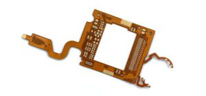
Rigid-flex PCBs represent a fascinating marriage of two distinct technologies. They integrate the structural integrity of traditional rigid boards with the dynamic flexibility of polyimide-based flexible circuits. This hybrid nature creates something greater than the sum of its parts—a circuit board that can bend, fold, and conform to three-dimensional spaces while maintaining the robust connection points and component mounting capabilities of rigid boards.
Think about the smartphone in your pocket. Inside, a rigid-flex PCB connects the display to the main logic board, folding elegantly to maximize space while eliminating fragile connectors that could fail. In telecommunications infrastructure, these boards enable optical transceiver modules to fit into compact housings while maintaining signal integrity across thousands of connection cycles. The beauty tech industry has embraced rigid-flex designs for wearable devices that must conform to body contours while housing complex electronics.
The advantages are compelling. By eliminating traditional connectors and cables, rigid-flex designs reduce weight by up to 60% compared to conventional multi-board systems. They shrink overall package size, improve reliability by reducing potential failure points, and enable product forms that simply aren’t possible with rigid-only solutions. For consumer electronics manufacturers, this translates to sleeker products. For industrial automation systems, it means equipment that survives harsh vibration environments. For augmented reality wearables, it enables the comfortable, lightweight designs users demand.
The Foundation: PCB Stackup Fundamentals
At its core, PCB stackup refers to the arrangement of copper and insulating layers that form your circuit board. But this simple definition belies enormous complexity. Each layer serves specific functions—signal routing, power distribution, ground planes—and their arrangement directly impacts electrical performance, thermal management, and mechanical integrity.
In industrial automation applications, where robust EMI shielding protects sensitive control signals from motor noise, proper ground plane placement within the stackup makes the difference between a system that works reliably and one that produces erratic behavior. Smart helmet designs for F1 racing and mining applications face similar challenges, requiring stackups that protect high-speed data transmission while withstanding extreme mechanical stress.
The stackup determines your board’s impedance characteristics, which govern signal integrity in high-speed designs. It affects crosstalk between adjacent traces, influences thermal dissipation, and dictates how well the board handles mechanical stress during both manufacturing and operation. Get the stackup wrong, and you’ll face signal degradation, electromagnetic interference issues, thermal hotspots, and premature mechanical failure.
For rigid-flex designs, stackup complexity multiplies. You’re not designing one board—you’re designing two interconnected systems combining rigid and flexible elements that must work seamlessly together while maintaining distinct mechanical properties. The rigid sections provide mounting stability and heat dissipation. The flexible sections enable movement and 3D packaging. Where they meet, careful transition design prevents stress concentration that could lead to failure.
Navigating Layer Configuration Complexity
In 2-12 layer rigid-flex designs, each additional layer exponentially increases design complexity. A simple two-layer flexible circuit offers basic signal routing with minimal complexity. Add power and ground planes, and you’re managing impedance control and EMI shielding. Scale to eight or twelve layers, and you’re orchestrating a symphony of signal layers, power distribution networks, and shielding planes—all while maintaining flexibility in designated areas.
Consider augmented reality wearables, where space constraints demand maximum functionality in minimal volume. These devices typically employ 6-8 layer stackups, with high-speed display interfaces on inner signal layers, power distribution on dedicated planes, and carefully routed sensor connections. The flexible sections, often just 2-4 layers, enable the board to wrap around the device frame while maintaining critical connections.
Drone manufacturers face different challenges. Their rigid-flex boards might use 4-6 layers, balancing weight constraints against the need for robust power distribution and signal routing. The rigid sections house heavy components and provide structural mounting points. Flexible sections snake through tight airframe spaces, eliminating the weight and failure risk of traditional cable harnesses.
Each layer serves a purpose, but that purpose differs between rigid and flexible sections. In flexible areas, you typically minimize layer count to maintain flexibility—often limiting to just signal and power/ground layers. Rigid sections can accommodate full layer stackups with multiple signal layers, dedicated ground planes, and power distribution networks. The challenge lies in transitioning smoothly between these different configurations without creating impedance discontinuities or mechanical stress points.
Material Selection: The Make-or-Break Decision
Material selection fundamentally determines your rigid-flex PCB’s success or failure. In flexible sections, polyimide reigns supreme for demanding applications. This remarkable material withstands temperatures from -200°C to +350°C, offers excellent chemical resistance, and maintains flexibility through hundreds of thousands of bend cycles. For rigid sections, FR-4 provides cost-effective mechanical stability and heat resistance.
But here’s where many designs fail: assuming all polyimides perform equally. They don’t. Different polyimide formulations offer vastly different properties. Some optimize for flexibility, others for thermal stability, still others for minimal moisture absorption. Beauty tech gadgets, which must survive bathroom humidity and repeated handling, require moisture-resistant polyimide formulations. Aerospace applications demand polyimides that maintain properties across extreme temperature swings.
Adhesive selection matters just as much. Traditional adhesive-based laminates introduce additional thickness and create potential delamination points under repeated flexing. Adhesive-less constructions, where polyimide bonds directly to copper, eliminate this failure mode while reducing overall thickness. For applications requiring tight bend radii or frequent flexing, adhesive-less materials aren’t optional—they’re mandatory.
The stiffener material that reinforces flexible sections for component mounting presents another critical choice. Polyimide stiffeners maintain flexibility characteristics while providing localized rigidity. FR-4 stiffeners offer superior dimensional stability but reduce overall flexibility. Stainless steel stiffeners provide maximum support for heavy components but add significant weight and cost.
Consider the trade-offs carefully. A medical device requiring sterilization cycles needs materials that survive repeated autoclaving. An electric vehicle application demands materials that handle wide temperature ranges and resist automotive fluids. Low-altitude airspace innovations like eVTOL vehicles need materials that maximize performance while minimizing weight. Each application demands thoughtful material selection aligned with real-world operating conditions.
Dynamic Bending: Designing for Movement
Static designs are simple. Dynamic designs that bend repeatedly during operation require entirely different thinking. The minimum bend radius—the tightest curve your flexible section can handle without damage—depends on multiple factors: material properties, copper weight, layer count, and expected bend cycles.
A general rule suggests minimum bend radius of six times the total flexible section thickness for dynamic applications involving frequent bending. Single-bend applications tolerate tighter radii. But these are starting points, not guarantees. Aerospace and defense applications, where reliability cannot be compromised, often specify even more conservative bend radii with substantial safety margins.
Trace routing through bend areas demands careful attention. Traces perpendicular to the bend axis experience maximum stress—like bending a wire back and forth until it breaks. Instead, route traces parallel to the bend axis whenever possible, or use curved routing that distributes stress more evenly. Staggered traces on different layers prevent stress concentration. Adequate spacing between traces accommodates the dimensional changes that occur during bending.
Copper thickness plays a crucial role. Thinner copper flexes more easily but limits current-carrying capacity. Rolled annealed copper flexes better than electrodeposited copper but costs more. Some designs use thicker copper in rigid sections for power distribution, transitioning to thinner copper in flexible sections to maintain flexibility—a technique that requires careful impedance management at transition points.
Real-world aerospace applications illustrate these principles perfectly. A satellite deployment mechanism might use rigid-flex boards with multiple 180-degree folds, designed for a single-use deployment in space. The board experiences one bending cycle—but it must work perfectly, in vacuum, across temperature extremes. Engineers specify generous bend radii, use rolled annealed copper, and route all traces parallel to fold lines. They test prototypes through thermal cycling and vibration testing that simulates launch conditions. This level of diligence ensures reliability when failure isn’t an option.
Manufacturing Constraints: Reality Meets Design
Even the most elegant design fails if manufacturers can’t build it reliably. Layer registration—the precise alignment of layers during lamination—becomes exponentially more challenging in rigid-flex designs. The flexible polyimide and rigid FR-4 sections expand and contract differently during processing. Variations in material properties, temperature cycles during lamination, and mechanical stresses during handling all contribute to alignment challenges.
Manufacturers typically specify registration tolerances around ±0.003 to ±0.005 inches for rigid-flex boards, though high-precision facilities achieve tighter tolerances. Your design must accommodate these realities. Via placement near rigid-flex transitions needs generous spacing. Fine-pitch components in flexible sections require careful consideration of achievable tolerances.
Stiffener placement and attachment present another manufacturing challenge. Stiffeners reinforce flexible sections for component mounting, but they create thickness transitions that complicate processing. Pressure-sensitive adhesives work for low-stress applications. Thermal bonding provides stronger attachment for demanding applications. Some designs incorporate stiffeners into the stackup during lamination, creating the most robust attachment but limiting future rework options.
Low-altitude airspace innovations showcase these manufacturing considerations perfectly. Drone flight controllers use rigid-flex boards with stiffeners precisely positioned to support connectors and mounting hardware. The boards must survive high vibration environments while maintaining signal integrity for flight-critical sensors and communications. Manufacturers employ precise stiffener placement, use thermal bonding for maximum reliability, and design generous tolerances for layer registration. They implement automated optical inspection to verify registration and stiffener placement before component assembly begins.
Edge treatments in flexible sections matter more than many designers realize. Standard routing operations can create rough edges that propagate cracks during flexing. Controlled depth routing, where tooling stops before penetrating completely through, produces smoother edges. Some designs specify laser cutting for flexible sections, eliminating mechanical stress from routing operations entirely.
Established Design Guidelines for Success
Success in rigid-flex PCB design requires following proven guidelines while adapting them to your specific application. Start with trace width calculations that account for both rigid and flexible sections. Flexible sections require wider traces than equivalent rigid sections for the same current-carrying capacity because polyimide dissipates heat less effectively than FR-4. Industry guidelines suggest increasing trace width by 25-30% in flexible sections compared to rigid sections for the same current load.
Grounding strategy becomes critical in mixed rigid-flex designs. Continuous ground planes provide excellent EMI shielding but reduce flexibility. Hatched or meshed ground planes maintain some shielding while preserving flexibility. The choice depends on your application’s EMI sensitivity versus flexibility requirements. Smartphone module designers often use solid ground planes in rigid sections for maximum shielding, transitioning to hatched grounds in flexible sections where bending occurs.
Component placement demands careful thought. Heavy or tall components belong in rigid sections where structural support is maximum. Components that must flex with the board require special mounting considerations—or perhaps suggest redesigning the layout to avoid components in flex areas entirely. Connectors face particular challenges; they concentrate mechanical stress and often become failure points if placed incorrectly.
Via design in flexible sections differs from rigid board practices. Through-vias create stress concentration points during bending, potentially causing failure. Staggered vias on different layers distribute stress better than aligned vias. Some designs avoid vias in high-flex areas entirely, routing signals on single layers through bend zones. When vias are unavoidable in flex sections, filled and capped vias provide the most reliable solution, though they add cost.
Thermal management requires special attention in rigid-flex designs. Components generate heat in rigid sections, but thermal conduction through flexible sections is limited. Polyimide’s thermal conductivity is roughly 10-20% of FR-4, and thin flexible sections offer limited heat spreading. Thermal vias help conduct heat from components into ground planes, but their effectiveness is limited in flexible sections with thin or hatched grounds. Some designs incorporate thermal interface materials or heat spreaders in rigid sections adjacent to high-power components.
Testing and validation before committing to production can save enormous expense. Prototype builds reveal manufacturing challenges early. Dynamic flex testing validates bend performance under realistic operating conditions. Thermal cycling identifies material compatibility issues. Vibration testing exposes mechanical weaknesses. Signal integrity measurements confirm electrical performance meets specifications. This investment in validation pays dividends by catching problems before they become production crises.
Pioneering the Future Through Stackup Mastery
Mastering rigid-flex PCB stackup design opens doors to innovations previously impossible. Electric vehicles advance when engineers design battery management systems that conform to complex vehicle geometries while handling high currents safely. Medical devices become less invasive when biocompatible flexible circuits fold into compact surgical instruments. Telecommunications infrastructure evolves as optical transceiver modules shrink while handling higher data rates.
The path forward demands both technical mastery and creative vision. Understanding material properties, respecting manufacturing constraints, and following proven design guidelines provide the foundation. But breakthrough innovations come from pushing boundaries thoughtfully—testing new materials, exploring novel stackup configurations, and validating designs thoroughly before committing to production.
Your 2-12 layer rigid-flex design won’t fail if you approach it with the comprehensive understanding these critical considerations provide. You’ll create products that survive real-world conditions, meet performance specifications, and push your industry forward. The electronic devices of tomorrow depend on designers who master today’s rigid-flex PCB challenges while envisioning what’s possible next.
The question isn’t whether rigid-flex technology will shape the future—it’s whether your designs will lead that transformation or follow it. With the right approach to stackup design, backed by thorough understanding of materials, manufacturing, and application-specific requirements, you position yourself at the forefront of electronic innovation. The complexity is real, but so is the opportunity for those who master it.