
In today’s miniaturized electronic world, where devices become smaller yet more powerful, flexible printed circuit boards (FPCBs) have emerged as the unsung heroes of modern design. These versatile circuit platforms bend, twist, and conform to three-dimensional spaces that rigid boards simply cannot accommodate. The art of flexible PCB production represents a perfect marriage of advanced materials science and precision engineering – a delicate balance that continues to push the boundaries of what’s possible in electronics manufacturing.
The Evolution and Impact of Flexible PCBs
Flexible PCBs have revolutionized electronic design across multiple industries. Unlike their rigid counterparts, these bendable circuits can be folded, twisted, and shaped to fit complex geometries, making them ideal for space-constrained applications. From the foldable displays in cutting-edge smartphones to the intricate circuitry in medical implants, flexible PCB production has become fundamental to innovation.
The impact of flexible circuits extends far beyond consumer electronics. In electric vehicle manufacturing, FPCBs power critical components like Head-Up Displays, wing mirrors, side CMS cameras, and LiDAR systems. Medical device manufacturers rely on biomedical-compatible flexible chip-on-board solutions for implantable devices and wearable health monitors. In the telecommunications sector, these flexible circuits enable compact, high-performance optical transceiver modules that form the backbone of our connected world.
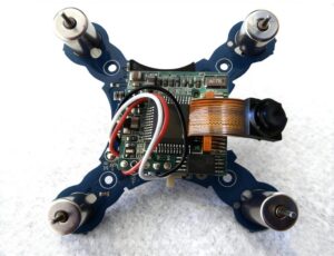
Perhaps most impressively, aerospace applications leverage the lightweight, reliable nature of flexible PCBs to reduce payload weight while maintaining mission-critical functionality. The low-altitude airspace sector – encompassing drones, eVTOL vehicles, air taxis, and aerial logistics – particularly benefits from the weight savings and design flexibility that FPCBs provide.
The Sophisticated Journey of Flexible PCB Manufacturing
The production of flexible PCBs involves a carefully orchestrated sequence of processes, each contributing to the final product’s reliability and performance. Understanding these stages reveals why flexible PCB production demands such specialized expertise.
The journey begins with material selection. Unlike rigid PCBs that typically use FR4 fiberglass, flexible circuits often employ polyimide as their base substrate. This remarkable material maintains electrical and physical properties while offering excellent heat resistance and mechanical flexibility. The copper foil used for conductive traces ranges from 18µm to 70µm, carefully selected based on the application’s current-carrying requirements. For more advanced applications, flexible COB technology enables even greater miniaturization possibilities.
Once materials are selected, the manufacturing process follows several critical steps:
1. Material Preparation: Copper-clad laminate sheets are cut to size and prepared for processing. For flexible PCB production, handling these thin, flexible materials requires specialized equipment to prevent damage.
2. Circuit Patterning: The circuit pattern is transferred to the copper through photolithography. A photoresist layer is applied, exposed through a film containing the circuit design, and developed to reveal areas where copper will remain.
3. Etching: Exposed copper areas are chemically removed, leaving only the desired circuit pattern. This chemical process must be precisely controlled to maintain line width and spacing tolerances as tight as 2/2mil.
4. Drilling and Via Formation: For multi-layer flexible PCBs, laser drilling creates precise vias that connect different layers. Unlike mechanical drilling used in rigid PCBs, laser drilling allows for smaller holes without mechanical stress.
5. Lamination: In multi-layer designs, separate circuit layers are aligned and bonded together with specialized adhesives or adhesiveless technologies that maintain flexibility while ensuring layer-to-layer reliability.
Each of these steps requires meticulous attention to detail and process control to ensure the final product meets stringent quality standards.
The Critical Nature of Process Controls in Flexible PCB Production
What truly distinguishes expert flexible PCB manufacturers from novices is their mastery of process controls. These quality assurance measures are the invisible guardians that ensure consistency, reliability, and performance across production runs.
1. Material Handling Controls
The thin, flexible nature of FPCB materials presents unique handling challenges. Leading manufacturers implement specialized material handling protocols to prevent damage, contamination, or deformation. Climate-controlled clean rooms maintain optimal temperature and humidity levels, while automated handling systems minimize human contact. These controls ensure material integrity from the moment raw materials enter the facility until finished products ship to customers. Failure to implement proper material handling controls can lead to significant yield loss and reliability issues downstream.
2. Imaging and Etching Precision Controls
The creation of circuit patterns demands extraordinary precision. Advanced manufacturers employ high-resolution imaging systems with automated optical alignment to achieve registration accuracy within microns. During etching, automated chemical process controls monitor and adjust solution chemistry, temperature, and agitation to maintain consistent line width and spacing. Statistical process control (SPC) data helps identify trends before they impact quality, ensuring that flexible PCB production maintains the 2/2mil precision that advanced applications demand. These precision controls are especially critical when implementing ±5° precision bonding technology for advanced flexible circuits.
3. Dimensional Stability Controls
One of the greatest challenges in flexible PCB production is maintaining dimensional stability of materials that are inherently designed to flex. Temperature and tension controls during lamination, along with specialized fixtures during processing, help minimize material movement. Leading manufacturers implement in-line dimensional verification using advanced optical measurement systems, comparing actual dimensions against design specifications to ensure that the final product will fit precisely in its intended application.
4. Contamination Prevention Controls
Even microscopic contamination can compromise flexible PCB reliability. World-class manufacturers maintain ISO Class 7 (10,000) or cleaner manufacturing environments, with specialized filtration systems, air showers, and cleanroom protocols. Materials undergo rigorous cleaning processes between manufacturing steps, and automated optical inspection (AOI) systems scan for particles or residues that could impact performance. Even a single particle can create an open or short circuit that compromises the entire board’s functionality.
5. Final Testing and Validation Controls
The ultimate process controls occur during final testing. High-potential (HiPot) testing verifies insulation integrity, while flying probe or bed-of-nails testing confirms electrical continuity and isolation. Advanced manufacturers also conduct flexibility testing, subjecting samples to thousands of flex cycles to verify mechanical durability. These comprehensive testing protocols ensure that only conforming products reach customers, providing confidence that the flexible PCB will perform reliably in the field.
Advanced Techniques Elevating Flexible PCB Design
Beyond basic process controls, innovative techniques in flexible PCB layout and construction continue to advance what’s possible in electronic design.
Adhesiveless materials represent one of the most significant innovations in flexible PCB production. By eliminating the traditional adhesive layer used to bond copper to polyimide, these materials offer superior thermal performance, improved dimensional stability, and enhanced reliability in extreme environments. The thinner overall construction also enables more flexible designs, critical for applications like foldable displays and wearable technology. According to industry fabrication guides, these advanced materials can reduce overall thickness by up to 30%.
Strategic use of stiffeners provides localized rigidity where components mount, while maintaining flexibility throughout the rest of the circuit. These stiffeners – typically made from FR4, polyimide, or metal – can be selectively applied to support connectors, components, or high-stress areas. Advanced manufacturers offer a variety of stiffener options, including laser-cut patterns that maintain partial flexibility even in reinforced areas.
Controlled impedance design techniques ensure signal integrity in high-frequency applications. By precisely controlling trace width, spacing, and dielectric thickness, manufacturers can achieve specific impedance values crucial for RF, high-speed digital, and telecommunications applications. This capability is particularly valuable in optical transceiver modules and advanced communication systems.
Rigorous Testing Ensures Reliable Performance
The final phase of flexible PCB production involves comprehensive testing to verify reliability under real-world conditions. These validation methods go far beyond simple continuity testing, subjecting circuits to the stresses they’ll encounter throughout their service life.
Environmental testing exposes flexible circuits to temperature extremes, humidity, and thermal cycling to verify performance across operating conditions. For automotive and aerospace applications, additional testing may include vibration, shock, and altitude simulation as outlined in aerospace PCB testing requirements. Medical devices undergo specialized biocompatibility testing to ensure safety for patient contact.
Reliability testing subjects samples to accelerated aging through techniques like highly accelerated life testing (HALT) and highly accelerated stress screening (HASS). These methods apply extreme stresses to identify potential failure modes before they occur in the field. By analyzing these results, manufacturers can continuously improve designs and processes.
Signal integrity testing verifies that high-speed signals maintain quality across the flexible circuit. Time-domain reflectometry (TDR) and vector network analysis measure impedance consistency and signal losses, ensuring that data-intensive applications like augmented reality wearables and AI glasses function flawlessly.
The Philosophy Behind Excellence in Flexible PCB Production
The meticulous processes and innovative techniques that define superior flexible PCB production align perfectly with Flex Plus (Xiamen) Co., Ltd’s philosophy of providing breakthrough flexible PCB solutions. Since 2004, this commitment to excellence has positioned Flex Plus as China’s leading certified flexible PCB and COB integration specialist.
What distinguishes true manufacturing excellence is the complete control of the production process. Unlike brokers or trading companies, a dedicated flexible PCB manufacturer maintains full oversight of every manufacturing step, from material selection through final testing. This comprehensive approach ensures consistent quality, enables rapid problem-solving, and provides the flexibility to adapt processes for unique customer requirements. Flex Plus exemplifies this comprehensive approach to flexible PCB manufacturing.
The integration of certified excellence, innovation, and complete manufacturing control creates a foundation for supporting diverse industry needs. From ultra-thin flexible PCBs with overall thickness as thin as 25 micron for medical devices to long format circuits extending up to 3 meters for industrial applications, specialized manufacturing capabilities open new possibilities for design engineers.
As electronics continue to evolve toward smaller, more flexible, and more capable devices, the hidden art of flexible PCB production becomes increasingly crucial to technological advancement. The five process controls highlighted here – material handling, imaging precision, dimensional stability, contamination prevention, and comprehensive testing – represent the foundation upon which tomorrow’s electronics will be built.
For design engineers pushing the boundaries of what’s possible, partnering with a flexible PCB manufacturer that masters these process controls isn’t just about producing circuits – it’s about enabling innovation itself. Through this partnership, the hidden art of flexible PCB production transforms from a manufacturing process into a catalyst for technological progress.