
In today’s high-stakes electronics industry, a single defect in a printed circuit board assembly can cascade into product recalls, safety hazards, or catastrophic system failures. For automotive manufacturers developing electric vehicles, medical device companies creating life-saving equipment, and aerospace contractors building mission-critical systems, zero-defect production isn’t just an aspirational goal—it’s a fundamental requirement. The question isn’t whether quality matters, but rather how manufacturers can systematically achieve defect-free production when scaling from prototypes to millions of units.
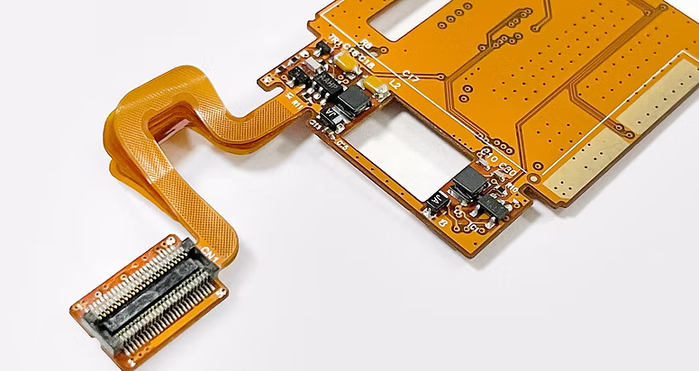
The challenge intensifies when working with flexible and rigid-flex PCBs, where mechanical stress, thermal dynamics, and material complexity create unique failure modes. A flexible circuit in a wearable medical device must withstand thousands of bending cycles without solder joint failure. An automotive sensor assembly must function flawlessly across temperature extremes from -40°C to 125°C. These demanding applications require more than occasional quality checks—they demand comprehensive process control embedded into every manufacturing stage.
The Critical Stages of PCB Assembly Manufacturing
PCB assembly manufacturing transforms bare circuit boards into functional electronic assemblies through a precisely orchestrated sequence of operations. Each stage presents specific opportunities for defects to emerge, making systematic process control essential.
The journey begins with design review and DFM analysis, where engineering teams evaluate whether a PCB design can be reliably manufactured at scale. At Flex Plus, this phase involves examining trace widths, pad geometries, component spacing, and substrate selection against our 20+ years of manufacturing data. A design might look perfect on CAD software but create yield issues during reflow soldering if thermal mass distribution isn’t properly balanced. By identifying these risks early, manufacturers prevent costly iterations and production delays.
Material procurement and inspection follows, where incoming components, substrates, and solder materials undergo rigorous verification. Counterfeit components remain a persistent industry problem, particularly in automotive and aerospace applications where component authenticity directly impacts safety. ISO 9001-certified material management systems track every component batch with full traceability, ensuring that moisture-sensitive devices receive proper handling and that substrate materials meet specified thickness tolerances.
Stencil design and solder paste application represents one of the most critical control points in surface mount technology (SMT) assembly. The stencil determines how much solder paste deposits onto each pad—too little creates weak joints prone to failure, while too much causes bridging defects between adjacent pads. Manufacturers optimize stencil aperture dimensions based on component pitch, pad geometry, and solder paste rheology. Solder Paste Inspection (SPI) systems then verify paste volume, height, and position before components are placed, catching deviations that would otherwise become defects downstream.
SMT component placement requires micron-level precision, especially for fine-pitch components like 0201 resistors or ball grid arrays (BGAs) with 0.4mm pitch. Modern pick-and-place machines achieve placement accuracy within ±0.025mm, but this precision means nothing without proper feeder management, nozzle maintenance, and vision system calibration. Statistical Process Control (SPC) monitors placement data in real-time, triggering alerts when machines drift outside acceptable parameters.
The reflow soldering process converts solder paste into metallurgical joints through a carefully controlled thermal profile. The temperature curve must reach sufficient peak temperature to create intermetallic bonds without exceeding the substrate’s glass transition temperature or damaging heat-sensitive components. For flexible PCBs, thermal management becomes even more complex because polyimide substrates conduct heat differently than rigid FR-4 material. Manufacturers develop substrate-specific reflow profiles and monitor them continuously with thermal profilers, ensuring consistent joint formation across every production panel.
Quality Control Methods That Drive Zero-Defect Production
Achieving zero-defect production at scale requires multiple inspection and testing methodologies working in concert, each targeting specific failure modes that could compromise product reliability.
Design for Manufacturability (DFM) checks form the first line of defense against quality issues. Rather than treating DFM as a one-time gate, leading manufacturers integrate it throughout the product lifecycle. When engineers at Flex Plus review a new rigid-flex design for an automotive application, we’re evaluating factors like bend radius in flexible sections, rigid-to-flex transitions that could create stress concentrations, and via-in-pad designs that require special filling processes. This proactive approach eliminates the root causes of defects before production begins.
IPC standards compliance provides the industry framework for quality acceptance. IPC-A-610, the acceptability standard for electronic assemblies, defines three classes of products with progressively stricter requirements. Class 3 products—used in aerospace, military, and medical applications—tolerate virtually no cosmetic or functional defects. The standard specifies exact criteria for solder joint appearance, component alignment, cleanliness, and workmanship. By adhering to IPC-A-610 Class 3 requirements, manufacturers establish objective quality thresholds that eliminate subjective interpretations of acceptability.
Similarly, J-STD-001 governs soldering processes and materials, detailing requirements for hand soldering, wave soldering, and reflow techniques. For automotive electronics, IATF 16949 adds layer-specific requirements around process failure mode analysis, production part approval, and continuous improvement. These standards aren’t bureaucratic overhead—they’re distilled wisdom from decades of industry experience with what actually prevents field failures.
Statistical Process Control (SPC) transforms quality from an inspection activity into a predictive science. Rather than discovering defects after they occur, SPC monitors key process parameters—like reflow oven temperature zones, placement force data, or AOI defect rates—and identifies trends before they produce nonconforming product. When a control chart shows increasing variance in solder paste volume measurements, technicians adjust printer parameters before the process drifts out of specification. This shift from reactive to predictive quality management dramatically reduces scrap rates while improving overall equipment effectiveness.
Automated inspection technologies provide the speed and consistency required for high-volume production. Solder Paste Inspection (SPI) examines every paste deposit in three dimensions, measuring volume within ±1% accuracy. Automated Optical Inspection (AOI) systems capture high-resolution images of assembled boards, using machine vision algorithms to detect missing components, tombstoned parts, insufficient solder, bridging, and component damage. X-ray inspection (AXI) reveals hidden defects in BGA packages, revealing voiding in solder balls, head-in-pillow defects, or insufficient wetting that AOI cannot see.
Each inspection technology targets specific defect types, which is why comprehensive quality control combines multiple methods. AOI excels at surface-level defects but cannot evaluate internal BGA connections. X-ray provides subsurface visibility but doesn’t verify correct component values. In-Circuit Testing (ICT) electrically validates component presence and values but requires test fixture costs that only make sense for volume production. Functional testing simulates real operating conditions but may not stress boards enough to expose latent defects. The optimal testing strategy balances coverage, cost, and production throughput based on product complexity and reliability requirements.
Technical Considerations That Impact Assembly Quality
Understanding the nuances of assembly technologies helps manufacturers optimize processes for different product requirements. The fundamental choice between SMT and through-hole technology illustrates this principle. Surface mount components offer higher density, better high-frequency performance, and automated assembly compatibility—but they’re more susceptible to mechanical stress and thermal cycling failure. Through-hole components provide superior mechanical strength, making them ideal for connectors subject to repeated insertion cycles or applications with significant vibration exposure.
Many designs use both technologies strategically. An automotive control module might employ SMT for most components while using through-hole mounting for high-current power connections or board-to-board connectors that require mechanical robustness. This mixed-technology approach demands careful process sequencing—typically SMT first, then selective wave soldering or hand soldering for through-hole components—to avoid thermal damage to already-assembled SMT components.
Solder paste selection and management profoundly impacts joint reliability. No-clean solder pastes eliminate cleaning process steps but leave residues that could cause issues in conformal coating applications. Water-soluble pastes enable thorough cleaning but require proper drying to prevent corrosion. Lead-free SAC305 alloy (96.5% tin, 3% silver, 0.5% copper) has replaced tin-lead solder in most applications, but its higher melting point and different wetting characteristics require process adjustments. For flexible PCB assembly, manufacturers must consider how repeated bending cycles affect solder joint fatigue life, often specifying specific paste alloys or reinforcement techniques for high-flex areas.
The thermal reflow profile represents perhaps the most critical process parameter in SMT assembly. A typical profile includes preheat (gradually warming components to prevent thermal shock), thermal soak (activating flux and reducing thermal gradients), reflow (melting solder to form joints), and cooling (solidifying joints with appropriate grain structure). For flexible substrates like polyimide, thermal profiling becomes more complex because the material’s lower thermal conductivity creates temperature differentials across the board. Large copper planes act as heat sinks, potentially preventing complete solder reflow in adjacent areas unless profile adjustments compensate. At Flex Plus, we develop substrate-specific thermal profiles validated through thermal profiling measurements and cross-sectional metallurgical analysis of joint formation.
Combining inspection and testing methodologies creates comprehensive defect coverage. Consider a multilayer rigid-flex assembly for a medical wearable device. SPI catches solder paste printing issues before components are placed. AOI after placement verifies correct component types and orientations. Post-reflow AOI detects solder defects and component damage. X-ray inspection examines BGAs and hidden solder joints in the rigid-flex transition zones. ICT validates proper electrical connectivity and component values. Finally, functional testing under simulated body temperature confirms the assembly operates correctly under realistic conditions. Each test catches defects that previous tests might miss, progressively filtering out nonconforming product before it reaches customers.
Flex Plus’s Integrated Approach to Zero-Defect Manufacturing
Achieving zero-defect production requires more than individual process controls—it demands systematic integration across the entire manufacturing value chain. At Flex Plus, our philosophy centers on three interconnected pillars: complete manufacturing control, engineering partnership, and certified excellence.
Complete manufacturing control means we maintain end-to-end ownership of production, eliminating the quality inconsistencies that plague broker-sourced PCBs. Our integrated FPCB assembly solutions streamline workflows from design through testing. When a design requires specialized processing—like our breakthrough flexible heat dissipation flow channels for thermal management or ultra-thin 25-micron flex circuits with gold plating—our 16,000+ square meter facility can execute these processes in-house with full traceability. Our engineers directly oversee substrate preparation, circuit imaging, etching, and finishing without relying on external subcontractors whose processes we cannot control. This vertical integration becomes especially critical for IATF 16949-certified automotive production, where every process parameter must be documented and controlled according to stringent automotive quality requirements.
Our engineering partnership approach recognizes that quality begins long before manufacturing starts. When a medical device manufacturer approaches us with a flexible COB design for a wearable biosensor, our applications engineers don’t just accept the design files—we conduct comprehensive DFMEA analysis examining potential failure modes. We evaluate whether the proposed die bonding approach will maintain our industry-leading wafer offset angle tolerance of ±5° across production volumes. We assess whether the flexible substrate requires our innovative magnetic fixture technology to prevent warping during encapsulation. We recommend dam encapsulation thickness specifications that balance protection with overall assembly thickness, leveraging our experience maintaining ±5μm dam thickness tolerance. This collaborative design optimization prevents quality issues by addressing root causes during development rather than discovering problems during production validation.
Certified excellence through international standards provides the framework ensuring consistent quality at scale. Our ISO 9001 certification establishes systematic quality management processes with documented procedures, corrective action systems, and management review cycles. ISO 13485 adds medical device-specific requirements around risk management, design controls, and regulatory compliance. IATF 16949 introduces automotive-specific tools like Advanced Product Quality Planning (APQP), Production Part Approval Process (PPAP), and Failure Mode Effects Analysis (FMEA) that drive continuous improvement. ISO 14001 environmental management ensures our processes minimize waste and environmental impact while maintaining quality. These aren’t separate initiatives—they’re integrated management systems that make quality improvement systematic rather than reactive.
Consider how these elements work together in volume production of automotive flexible circuits. A Tier 1 supplier needs 500,000 pieces monthly of a 4-layer rigid-flex assembly for EV battery management systems. The design undergoes detailed DFM review, identifying areas where trace routing could affect impedance matching and where rigid-to-flex transitions should be reinforced for vibration resistance. Material procurement follows IATF 16949 requirements with approved supplier lists and incoming material verification. Production uses our roll-to-roll processing capabilities for high-volume efficiency, with inline SPI, AOI, and electrical testing catching defects in real-time. Statistical process control monitors dozens of parameters across SMT placement, reflow, and inspection operations, triggering immediate investigation when any parameter trends toward control limits. Every production lot receives PPAP-compliant documentation including dimensional verification, material certifications, and performance test results. This systematic approach consistently delivers automotive-grade quality at production scale.
Building Your Path to Zero-Defect Production
For professionals tasked with sourcing PCB assembly solutions that meet uncompromising quality requirements, several key principles separate reliable partners from those who merely claim capability.
First, demand direct manufacturing control rather than broker relationships. When quality issues arise—and they inevitably do even in well-controlled processes—direct access to production engineers accelerates root cause analysis and corrective action. Brokers add communication layers that slow problem resolution and obscure who actually controls the manufacturing process.
Second, verify authentic certifications matched to your application. An ISO 9001 certificate proves basic quality management, but medical devices require ISO 13485 compliance, automotive applications need IATF 16949, and aerospace often demands AS9100. These aren’t interchangeable—each standard addresses industry-specific failure modes and regulatory requirements. Request certificate numbers and verify them through registrar databases rather than accepting copies that could be outdated or fraudulent.
Third, insist on comprehensive process documentation and traceability. Zero-defect production depends on knowing exactly which material lot, equipment setup, and process parameters produced every assembly. Ask potential manufacturers about their Material Review Board processes for handling nonconforming material, their corrective action response times, and their systems for process change control. Companies with mature quality systems can readily provide this documentation because it’s embedded in their daily operations.
Fourth, evaluate technical capabilities beyond standard offerings. As products become more compact and performance-demanding, assembly challenges intensify. Flexible substrates that must survive thousands of bending cycles, ultra-thin profiles that demand specialized handling, or thermal management requirements for high-power applications require proven expertise. Manufacturers who’ve solved these challenges in volume production—like Flex Plus‘s COB integration capabilities with micron-level precision packaging—bring valuable problem-solving experience that prevents costly learning curves on your product.
Finally, recognize that zero-defect production is a journey requiring continuous improvement. No manufacturer achieves perfection immediately—what matters is their systematic approach to identifying and eliminating defect sources. Companies that openly discuss their quality metrics, improvement initiatives, and lessons learned from past challenges demonstrate the transparency and commitment that characterize reliable long-term partners.
The electronics industry’s relentless push toward miniaturization, higher reliability, and lower costs makes quality management increasingly complex. But manufacturers who integrate rigorous process control, multiple inspection technologies, international standard compliance, and genuine engineering partnership create the foundation for zero-defect production at scale. For the engineers, procurement specialists, and quality professionals responsible for ensuring product success, selecting a manufacturing partner with these capabilities isn’t just about current production needs—it’s about building the relationship that enables your next generation of innovation.