
The electronics industry stands at a crossroads. As devices become smaller, lighter, and more powerful, traditional rigid printed circuit boards simply cannot meet the demands of modern applications. Enter flexible PCB assembly—a revolutionary technology that’s transforming everything from electric vehicle sensors to life-saving medical devices. Yet despite its promise, a staggering 90% of flexible PCB projects encounter critical failures that derail timelines, inflate budgets, and compromise product quality.
Consider the electric vehicle manufacturer racing to integrate advanced Head-Up Display systems, only to discover their flexible circuits cracking at bend points during testing. Or the medical device company facing regulatory rejection because their biocompatible flex PCB assembly failed to meet ISO 13485 standards. These aren’t isolated incidents—they’re symptoms of a fundamental gap between ambition and execution in flexible PCB assembly.
The stakes couldn’t be higher. In aerospace and defense applications, a single assembly failure can compromise mission-critical systems. For telecommunications companies deploying next-generation infrastructure, unreliable flexible circuits mean network downtime and lost revenue. And in the rapidly expanding world of drones, eVTOL vehicles, and air taxis operating in low-altitude airspace, assembly defects can have life-threatening consequences.
The Hidden Traps That Sink Flexible PCB Projects
Most flexible PCB assembly failures don’t announce themselves with dramatic explosions or sparks. Instead, they creep in quietly through three insidious categories that catch even experienced engineers off guard.
Material Selection: The Foundation That Makes or Breaks Your Project
The materials you choose for your flexible PCB assembly aren’t just specifications on a datasheet—they’re the difference between success and catastrophic failure. Too many projects stumble because designers apply rigid PCB thinking to flexible applications, selecting polyimide substrates without considering the specific mechanical stresses their application will face.
A leading beauty tech company learned this lesson the hard way. Their innovative hair styling device required a flexible circuit that could withstand repeated bending cycles while maintaining signal integrity. They initially chose standard polyimide with copper foil, only to discover delamination after just 500 bend cycles—far short of the 100,000 cycles their product required. The culprit? Inadequate adhesive systems between the copper layer and polyimide substrate.
The material challenge extends beyond just the substrate. Coverlay selection, adhesive types, stiffener placement, and copper foil thickness all interact in complex ways. A rigid-flex design for an F1 racing smart helmet might require specific flame-retardant materials that can withstand extreme temperatures, while a medical wearable demands biocompatible materials that won’t trigger adverse reactions.
Design Considerations: Where Theory Meets Physical Reality
Flexible PCB design isn’t simply about routing traces on a flexible substrate. It requires understanding how circuits behave when bent, twisted, and flexed thousands of times. Yet countless projects proceed with designs that look perfect in CAD software but fail within minutes of physical testing.
The bend radius represents perhaps the most critical—and most frequently violated—design parameter. When a flexible PCB bends too sharply, copper traces stretch on the outer radius and compress on the inner radius, creating stress concentrations that lead to cracking and open circuits. Industry standards specify minimum bend radios based on the overall stack-up thickness, yet designers routinely ignore these guidelines in pursuit of tighter packaging.
Transition zones between rigid and flexible sections present another common failure point. A manufacturer of AR wearables discovered their glasses-mounted display flickering intermittently during user trials. The root cause? Improper stiffener placement at the rigid-flex boundary created stress concentrations that fractured copper traces during normal head movements. What seemed like a minor design detail became a showstopper requiring complete redesign.
Via placement in flexible regions demands special attention too. Standard through-hole vias that work perfectly in rigid PCBs become crack initiation points when subjected to bending stresses. Successful flexible PCB designs either avoid vias in dynamic flex regions entirely or utilize specialized tear-drop via designs that distribute stress more evenly.
Precision in Component Placement and Soldering: The Make-or-Break Moment
Even with perfect materials and flawless design, flexible PCB projects fail at the assembly stage more than anywhere else. The delicate nature of flexible substrates, combined with the precision required for modern component sizes, creates a minefield of potential failures.
Surface mount technology on flexible PCBs differs fundamentally from rigid board assembly. The substrate’s flexibility means traditional vacuum hold-down systems can create localized deformation, throwing component placements out of alignment by critical microns. A telecommunications equipment manufacturer producing optical transceiver modules faced exactly this challenge—their initial assembly runs showed unacceptable component misalignment rates exceeding 15%, far above their 0.1% target.
Soldering flexible PCBs presents its own unique challenges. The polyimide substrate has different thermal expansion characteristics than rigid FR-4, meaning solder reflow profiles optimized for rigid boards can cause warping, component tombstoning, or insufficient solder joint formation. Temperature gradients across flexible assemblies can be particularly problematic, with thin flexible regions heating much faster than reinforced areas.
Then there’s the human factor. Operators accustomed to handling rigid boards often apply excessive pressure during manual assembly steps, creating creases or stress points that won’t manifest as failures until after the product reaches customers. An industrial control system integrator discovered this when field failures spiked six months after product launch—subtle handling damage during assembly had created latent defects that only appeared after thermal cycling in actual use.
The Critical Steps That Separate Success From Failure
Surviving the flexible PCB assembly gauntlet requires methodical attention to specific steps that successful manufacturers implement without compromise.
Meticulous Design Planning: Engineering Success From Day One
The most successful flexible PCB projects begin long before the first circuit is fabricated. They start with comprehensive Design for Manufacturing (DFM) analysis that examines every aspect of the design through the lens of manufacturing reality.
A DFM review for flexible PCBs goes beyond the standard checks performed for rigid boards. It includes finite element analysis of bend stresses, thermal simulation of reflow profiles across mixed rigid-flex stackups, and mechanical modeling of connector strain relief. This upfront investment catches 90% of potential assembly issues before they become expensive manufacturing problems.
Material consultation represents another critical early step. Rather than designers specifying materials in isolation, successful projects involve materials engineers who understand the interplay between substrate properties, adhesive systems, and manufacturing processes. When a medical device company needed ultra-thin flexible circuits for an implantable device, materials experts recommended a specific polyimide grade with enhanced tear resistance and a specialized adhesiveless construction that reduced overall thickness while improving reliability.
Layer stackup optimization deserves particular attention in multilayer flexible designs. Each additional layer increases complexity exponentially, so successful designs ruthlessly eliminate unnecessary layers while strategically placing copper traces to minimize crosstalk and impedance variations. The goal isn’t just electrical performance—it’s creating a stackup that can be manufactured consistently at volume without yield-killing defects.
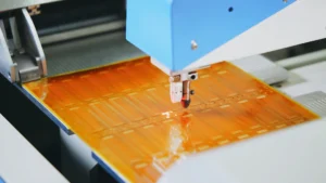
Specialized SMT Equipment: The Technology That Makes Precision Possible
Assembling flexible PCBs with equipment designed for rigid boards is like performing brain surgery with a butcher knife—technically possible but practically inadvisable. Purpose-built flexible PCB assembly equipment makes the difference between acceptable and exceptional yields.
Modern SMT lines optimized for flexible PCB assembly incorporate several key technologies. Vacuum fixtures specifically designed for flexible substrates provide support without inducing stress or deformation. These fixtures often use thousands of small vacuum holes distributed across the support surface, creating even pressure that conforms to the flexible circuit’s natural form.
Vision alignment systems require higher precision for flexible PCB assembly because substrate deformation can throw fiducial marks out of position relative to component pads. Advanced systems use multiple camera angles and AI-driven pattern recognition to compensate for substrate variations, achieving placement accuracy within ±25 microns even on challenging flexible substrates.
Component placement heads designed for flexible work differ from standard SMT nozzles. They apply controlled downward force with force feedback, preventing the excessive pressure that can damage flexible substrates while ensuring proper component seating. A smartphone module manufacturer implementing force-controlled placement reduced their component damage rate from 3% to less than 0.1%, directly improving their bottom line.
Reflow ovens for flexible PCB assembly require precise temperature profiling capabilities. The ideal system provides independent zone control allowing different heating and cooling rates for areas with varying thermal mass. This prevents the warping that plagues flexible assemblies heated with standard reflow profiles designed for rigid boards.
Robust Quality Assurance Measures: Catching Problems Before They Reach Customers
Quality assurance in flexible PCB assembly goes far beyond basic electrical testing. It requires comprehensive inspection strategies that catch mechanical defects, latent failures, and workmanship issues that might not be immediately apparent.
Automated Optical Inspection (AOI) systems designed for flexible circuits must account for the substrate’s tendency to have slight variations in flatness and position. Three-dimensional AOI systems that build complete topographical maps prove most effective, identifying solder joint defects, component placement errors, and substrate damage that two-dimensional systems miss.
Electrical testing takes on added complexity with flexible circuits. Standard flying probe testers struggle with flexible substrates that deflect under probe pressure. Successful manufacturers employ either fixture-based testing with carefully designed support structures or advanced flying probe systems with force-calibrated probes that compensate for substrate flexibility.
But the most critical quality assurance step is dynamic flex testing—actually flexing assembled circuits through their designed range of motion while monitoring for electrical failures. This catches intermittent connection problems, trace cracking, and component attachment issues that static testing misses entirely. An EV manufacturer implementing comprehensive flex testing during assembly caught design flaws in their camera module flex circuits that would have caused field failures after just months of vehicle operation.
Environmental stress screening takes flexible PCB quality assurance to the next level. By subjecting assemblies to accelerated thermal cycling, vibration, and humidity exposure, manufacturers identify latent defects before they reach customers. This “burn-in” approach costs more upfront but dramatically reduces warranty claims and field failures.
Advanced Technologies That Push Performance Boundaries
The cutting edge of flexible PCB assembly extends beyond traditional methods, embracing advanced integration techniques that deliver unprecedented performance in the most demanding applications.
Chip-on-Board (COB) integration represents perhaps the most significant advancement in flexible PCB technology. By mounting bare semiconductor dies directly onto flexible substrates, COB eliminates the packaging overhead of traditional integrated circuits, enabling ultra-thin designs impossible with conventional surface mount components.
The precision required for COB on flexible substrates exceeds even the demanding standards of rigid board assembly. Die bonding must achieve placement accuracy within ±5 microns while accounting for the flexible substrate’s thermal expansion during the bonding process. Advanced manufacturers have developed magnetic fixture technologies that stabilize flexible substrates during die attach, solving the challenge of non-planar surfaces that plagued early COB attempts.
Wire bonding onto flexible substrates requires specialized approaches too. The substrate must be rigidly supported during the bonding process to prevent deformation from the bonding tool’s ultrasonic energy, yet this support must be removable without damaging the delicate flexible circuit. Successful COB integration on flexible substrates depends on purpose-designed tooling that can support the substrate during bonding then release cleanly afterward.
Encapsulation of COB assemblies on flexible substrates presents unique challenges. The encapsulant must protect the delicate wire bonds and die surfaces while maintaining the flexibility required for the application. Dam and fill processes achieve encapsulation thickness tolerances of ±5 microns, creating protective layers that flex with the substrate without cracking or delaminating.
The advantages of COB integration on flexible substrates are transformative for applications requiring ultimate miniaturization. Medical wearables achieve sensor package thicknesses below 100 microns—thinner than two sheets of paper. AI-powered glasses integrate complete display drivers directly onto flexible circuits, eliminating connectors and reducing weight by 40%. These aren’t incremental improvements; they’re generational leaps enabled by advanced flexible PCB assembly techniques.
High-density interconnect (HDI) technology further extends flexible PCB capabilities. Utilizing microvias with diameters as small as 75 microns, HDI flexible circuits pack more functionality into smaller areas while maintaining impedance control essential for high-speed signals. The combination of HDI and COB creates flexible assemblies with component densities approaching those of rigid boards while retaining full flexibility.
Transparent flexible PCBs represent an emerging application area where advanced assembly techniques enable entirely new product categories. Using transparent conductive materials like indium tin oxide on clear polyimide substrates, these circuits disappear into their applications. But assembling traditional opaque components onto transparent substrates requires specialized placement equipment with through-substrate vision capabilities.
Engineering Partnership: The Philosophy Behind Reliable Flexible PCB Solutions
At the foundation of every successful flexible PCB assembly project lies a fundamental truth: technical excellence alone isn’t enough. The complexity of modern flexible circuits demands true engineering partnerships between designers and manufacturers, built on principles of certified quality, complete manufacturing control, and collaborative innovation.
Certified excellence isn’t just about displaying certificates on a wall—it’s about embedding quality systems into every process step. ISO 9001 ensures consistent processes, but ISO 13485 specifically addresses the unique requirements of medical device manufacturing where biocompatibility and traceability become paramount. IATF 16949 certification proves capability to meet automotive industry quality standards, essential for EV manufacturers whose products must survive years of thermal cycling, vibration, and environmental exposure. Adherence to IPC-6013 standards ensures flexible circuits meet internationally recognized performance criteria.
These certifications matter because they represent systematic approaches to catching problems before they become failures. A certified quality system means that when an aerospace manufacturer requires documentation proving every material lot used in their flight-critical flexible assemblies, complete traceability exists. When a medical device company needs validation of biocompatibility for implantable flexible circuits, certified processes provide the evidence regulators demand.
Complete manufacturing control distinguishes real flexible PCB factories from brokers and trading companies. When manufacturing happens in-house, engineering feedback loops close in hours instead of weeks. A design question gets answered by walking across the factory floor to consult with production engineers who have hands-on experience with the exact processes involved. Prototype iterations happen in days because there’s no waiting for external vendors. Quality issues get root-caused immediately because the people who built the circuits are available to examine failures and implement corrections.
This vertical integration proves especially valuable for rapid prototyping. Engineers developing next-generation drone electronics need iterative prototyping cycles measured in days, not weeks. When design, fabrication, and assembly all occur under one roof, these accelerated timelines become achievable. Emergency requests that would be impossible through broker channels become routine when dealing with a vertically integrated manufacturer.
Engineering partnership means involving manufacturing expertise from the earliest design stages. Rather than designers working in isolation then throwing designs over the wall to manufacturing, successful projects integrate manufacturing knowledge into design decisions from day one. This collaborative approach prevents the expensive redesign cycles that plague projects where manufacturability becomes an afterthought.
The philosophy extends to environmental responsibility through ISO 14001 certification, demonstrating that manufacturing excellence and environmental stewardship aren’t competing priorities but complementary goals. As electronic products proliferate into every aspect of modern life, manufacturers bear responsibility for minimizing their environmental footprint while delivering the innovative solutions customers demand.
From Vision to Reality: Reliable Flexible PCB Solutions
The path from flexible PCB concept to successful product demands more than technical capability—it requires partnership with manufacturers who understand the complete product lifecycle from initial consultation through high-volume production.
Comprehensive design support begins at the concept stage, where experienced engineers help customers evaluate whether flexible PCBs represent the optimal solution for their application. Sometimes rigid-flex combinations prove more cost-effective. Other times, pure flexible designs deliver superior performance. Honest technical consultation saves customers from expensive missteps.
Material consultation ensures designs use substrate combinations optimized for their specific requirements. An eVTOL vehicle manufacturer’s camera module requires polyimide with specific thermal stability characteristics. A beauty tech wearable needs materials that feel pleasant against skin while surviving repeated flexing during use. Smart helmet displays demand flame-retardant materials meeting stringent safety standards. Each application has unique requirements that generic material selections don’t address.
The progression from prototyping through engineering samples to mass production benefits from streamlined processes when working with vertically integrated manufacturers. Prototypes validate design concepts. Engineering samples undergo comprehensive testing including dynamic flex cycling, thermal stress screening, and electrical characterization. Lessons learned feed back into design refinements before committing to production tooling. This staged approach minimizes risk while accelerating time-to-market.
Full assembly services including component sourcing, SMT assembly, and comprehensive testing reduce vendor complexity. Rather than coordinating between PCB fabricators, assembly houses, and test facilities, customers work with a single engineering team that understands their product holistically. This consolidated approach reduces communication overhead, eliminates finger-pointing when issues arise, and ensures accountability from design through delivery.
For applications demanding ultimate miniaturization, COB integration provides capabilities unmatched by traditional assembly approaches. Direct die attachment achieves package thicknesses and form factors impossible with packaged components. This technology proves essential for applications from medical implants to AR wearables where every micron matters.
Global reach combined with local expertise allows manufacturers to support customers across North America, Europe, Asia, and beyond while maintaining consistent quality standards. Time zone challenges dissolve when engineering teams provide round-the-clock support. Cultural and language barriers fade when working with experienced international manufacturers who understand diverse customer needs.
The specialized expertise developed through thousands of successful projects across multiple industries means manufacturers can anticipate challenges before customers encounter them. An industrial automation customer benefits from lessons learned building medical devices. A telecommunications equipment manufacturer leverages design principles proven in automotive applications. This cross-pollination of knowledge accelerates development and improves reliability.
The Future Belongs to Those Who Execute Correctly
As electronics continue their relentless march toward smaller, lighter, and more capable devices, flexible PCB assembly will only grow in importance. The technologies enabling tomorrow’s innovations—from urban air mobility to bioelectronic medicine to ubiquitous augmented reality—all depend on flexible circuits assembled with precision and reliability.
But success in this demanding field requires more than enthusiasm and good intentions. It demands meticulous attention to material selection, comprehensive design planning, specialized equipment, robust quality systems, and advanced integration techniques. Most critically, it requires partnership with manufacturers who possess both technical capability and systematic approaches to quality proven through rigorous certification.
The 90% of projects that fail do so not because flexible PCB assembly is impossibly difficult, but because they skip critical steps, compromise on quality, or partner with manufacturers lacking the necessary expertise and infrastructure. The 10% that succeed recognize that flexible PCB assembly represents not just a manufacturing process but an engineering discipline requiring specialized knowledge, purpose-built equipment, and unwavering commitment to quality.
For engineers and companies embarking on flexible PCB projects, the choice is clear: invest the time and resources to execute correctly from the start, or join the 90% learning expensive lessons through failure. The difference between success and failure often comes down to asking the right questions early, demanding certified quality systems, insisting on complete manufacturing control, and partnering with manufacturers who view customer success as their own.
In an industry where a single assembly defect can ground an aircraft, endanger a patient, or strand a vehicle, there’s no substitute for doing things right the first time. The critical steps outlined here aren’t optional enhancements—they’re the foundation upon which reliable flexible PCB assembly is built. Master them, and you’ll join the elite 10% who consistently deliver projects on time, on budget, and with the quality modern applications demand.