
Ever wonder how your smartphone bends without breaking? Or how medical devices pack so much technology into such tiny spaces? The answer lies in a remarkable innovation that most people never see: flexible printed circuit boards (flex PCBs). These bendable marvels of engineering are the unsung heroes powering the sleek, compact electronic devices we rely on daily.
The Revolutionary Role of Flex PCBs in Modern Electronics
Flexible PCBs represent one of the most significant advancements in modern electronics manufacturing. Unlike their rigid counterparts, flex PCBs can bend, fold, and twist to conform to irregular shapes and tight spaces. This flexibility isn’t just convenient—it’s revolutionary.
The importance of flex PCBs in today’s electronics cannot be overstated. Their ability to fit into compact and irregularly shaped spaces has transformed product design across multiple industries. In electric vehicles, flex PCBs enable sophisticated dashboard displays and critical sensor systems while reducing weight—a crucial factor in extending range and efficiency. In medical devices, they make possible the miniaturization of life-saving equipment, from pacemakers to hearing aids. The aerospace industry relies on flex PCBs to withstand extreme vibrations and save valuable weight in aircraft and satellites.
What makes flex PCBs truly special is their combination of reliability and adaptability. Their inherent elasticity allows them to absorb shocks and vibrations better than rigid boards, making them ideal for applications where durability is essential. By eliminating the need for multiple connectors and cables, flex PCB fabrication reduces potential points of failure, enhancing overall system reliability.
The evolution of flexible circuit technology marks a major leap forward in electronics, allowing designers to break free from the constraints of traditional PCB designs. As devices continue to shrink while adding functionality, high-quality flexible PCBs have become not just useful but essential components in modern electronic design.
Critical Design Considerations for Flex PCB Success
Creating effective flex PCBs requires careful consideration of several key factors that influence their performance, durability, and cost-effectiveness.
Understanding Bending Requirements
The most fundamental consideration in flex PCB design is understanding exactly how and where the circuit will bend. Engineers must carefully analyze:
- Bend radius: The minimum bend radius determines how tightly the PCB can flex without damage. Smaller bend radii require special design considerations.
- Static versus dynamic bending: Some flex PCBs bend once during installation and remain fixed (static), while others must withstand repeated bending throughout their lifecycle (dynamic).
- Bend zones: Proper designation of bend zones ensures components and traces aren’t placed where flexing occurs, preventing stress and failure.
Material Selection: The Foundation of Performance
Material choice directly impacts a flex PCB’s performance characteristics:
- Polyimide substrates are the industry standard for flex PCBs, offering excellent thermal stability and mechanical durability. For applications requiring biocompatibility, like medical devices, specialized materials such as TPU (thermoplastic polyurethane) may be used.
- Copper type and thickness significantly affect both flexibility and electrical performance. Thinner copper improves flexibility but increases electrical resistance.
- Adhesives versus adhesiveless laminates: Adhesiveless constructions typically offer better dimensional stability and heat resistance, which is critical for high-temperature applications in automotive and aerospace environments.
Stack-Up Configuration
The layer structure of a flex PCB dramatically influences its flexibility and functionality:
- Single-sided flex offers maximum flexibility but limited circuit complexity
- Double-sided flex provides more routing options while maintaining good flexibility
- Multilayer flex supports complex circuitry but with reduced flexibility
- Rigid-flex combinations integrate rigid and flexible sections to optimize both space and performance
Copper Feature Placement and Routing
Strategic copper placement is essential for reliable flex PCB performance:
- Trace routing perpendicular to bend lines minimizes stress on connections
- Staggered via placement in transition zones prevents cracking
- Hatched ground planes rather than solid copper improve flexibility while maintaining electrical performance
- Rounded corners on traces reduce stress concentration points
Cost Considerations
While flex PCBs offer tremendous advantages, they typically cost more than rigid boards. Cost optimization strategies include:
- Minimizing layer count when possible
- Utilizing standard material thicknesses
- Optimizing panel utilization during manufacturing
- Balancing flexibility requirements with cost constraints
By carefully addressing these design considerations, engineers can create flex PCBs that meet the demanding requirements of today’s advanced electronic devices while ensuring reliability and manufacturability.
The Art and Science of Flex PCB Fabrication
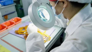
The manufacturing process of flexible PCBs combines precision engineering with advanced materials science. Understanding this process reveals why flex PCB fabrication requires specialized expertise and equipment.
Material Preparation and Handling
The manufacturing journey begins with the preparation of base materials, typically polyimide films coated with copper. Unlike rigid PCBs, these materials are extremely thin and require special handling to prevent damage. The base material is typically delivered in roll form and must be carefully cut to size and stabilized for processing.
Photolithography: Creating the Circuit Pattern
The circuit pattern is transferred to the copper through a photolithographic process:
1. A photoresist layer is applied to the copper surface
2. The circuit pattern is projected onto the photoresist using precision optical equipment
3. The exposed areas are developed, leaving a protective mask in the pattern of the desired circuit
4. For flex PCBs, this process requires extremely precise alignment due to the thin, flexible nature of the substrate
Etching: Defining the Conductive Paths
Once the pattern is created, the unprotected copper is removed through chemical etching:
1. The material is exposed to chemical etchants that dissolve unmasked copper
2. The etching process must be carefully controlled to maintain precise line widths and spacing
3. For high-density flex PCBs, the etching parameters become even more critical due to the fine feature sizes
Layering and Lamination for Multi-Layer Flex PCBs
For multi-layer flex PCBs, the individual layers must be precisely aligned and bonded:
1. Alignment holes are created in each layer to ensure proper registration
2. Specialized adhesives or bonding films join the layers under precise heat and pressure conditions
3. The lamination process must maintain the flexibility of the final product while ensuring reliable connections between layers
Creating Via Connections
Electrical connections between layers are created through vias:
1. Laser drilling is often preferred for flex PCBs due to its precision and minimal mechanical stress
2. The via holes are then metalized through chemical deposition processes
3. Special attention must be paid to via reliability in bend areas
Surface Finishing and Protection
The completed circuit requires protection against environmental factors:
1. A coverlay (similar to solder mask in rigid PCBs) is applied to protect the circuits
2. Surface finishes like ENIG (Electroless Nickel Immersion Gold) or OSP (Organic Solderability Preservatives) are applied to connection pads
3. For flex PCBs, these protective layers must maintain flexibility while providing reliable protection
Final Processing and Testing
Before delivery, the completed flex PCBs undergo:
1. Electrical testing to verify connectivity and isolation
2. Bend testing for flexible areas
3. Final inspection for dimensional accuracy and visual defects
The manufacturing process for flex PCBs demands specialized equipment, controlled environments, and expertise in handling delicate materials. This precision fabrication ensures the reliability and performance that modern electronic devices require.
Diverse Applications Across Industries
The unique capabilities of flex PCBs have enabled remarkable innovations across numerous industries, driving technological advancement in ways that would be impossible with conventional rigid boards.
Consumer Electronics Revolution
In consumer electronics, flex PCBs have enabled the dramatic reduction in size and weight of everyday devices:
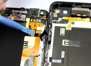
- Smartphones utilize flex PCBs to connect displays, cameras, speakers, and other components while fitting into increasingly slim profiles
- Wearable technology like fitness trackers and smartwatches rely on flex PCBs to conform to the human body
- Foldable display technologies in modern devices would be impossible without advanced flex PCB designs
Medical Device Innovations
The medical field has seen transformative applications of flexible COB technology:
- Implantable devices like pacemakers and neurostimulators utilize biocompatible flex PCBs to achieve smaller sizes and conform to human anatomy
- Hearing aids have shrunk dramatically thanks to flex circuits that fit into the ear canal
- Medical imaging equipment uses flex PCBs to connect moving parts while maintaining signal integrity
Automotive Advancements
Modern vehicles increasingly depend on flexible chip-on-board solutions:
- Electric vehicle systems utilize flex PCBs for battery management, display systems, and sensor networks
- Advanced driver assistance systems (ADAS) rely on flex PCBs to connect cameras, radars, and control modules
- Dashboard displays and infotainment systems leverage flex PCBs to fit into complex interior designs
Aerospace and Defense Applications
The demanding requirements of aerospace and defense applications are well-suited to flex PCB capabilities:
- Satellite systems benefit from the weight reduction and reliability of flex PCBs
- Aircraft avionics use flex PCBs to withstand vibration while saving weight
- Military equipment leverages flex PCBs for portable and ruggedized electronics
Emerging Technologies
Flex PCBs are enabling entirely new categories of technology:
- Low-altitude airspace innovations like drones and electric vertical takeoff and landing (eVTOL) vehicles
- Augmented reality wearables and AI glasses that conform to human facial features
- Smart helmets for applications ranging from F1 racing to mining operations
These diverse applications demonstrate how flex PCB fabrication has become indispensable to modern electronics, enabling innovation across industries by overcoming the limitations of traditional rigid boards.
Excellence in Flex PCB Solutions: The Flex Plus Approach
The world of flexible PCBs continues to evolve rapidly, with new applications emerging across industries. As technology advances, the expertise required to design and manufacture these sophisticated circuits becomes increasingly specialized.
Flex Plus (Xiamen) Co., Ltd stands at the forefront of this technological evolution as China’s leading certified flexible PCB and COB integration specialist. With over 20 years of experience since 2004, Flex Plus has developed unparalleled expertise in creating high-performance flexible circuits that power innovation across diverse industries.
What distinguishes Flex Plus in the flex PCB fabrication landscape is its comprehensive approach to quality and innovation. The company maintains stringent certification standards, including ISO 9001, ISO 13485 for medical devices, and IATF 16949 for automotive applications, ensuring that every flexible circuit meets the highest international quality benchmarks.
Innovation drives the Flex Plus philosophy. The company’s advanced R&D capabilities have pioneered breakthrough technologies like flexible heat dissipation flow channels, transparent PCBs, and ultra-thin designs with overall thickness as thin as 25 microns on double-sided flex PCBs. These innovations enable customers to push the boundaries of what’s possible in electronic design.
Unlike brokers or trading companies, Flex Plus maintains complete manufacturing control with an 8,000+ square meter factory equipped with advanced production lines. This direct manufacturing capability ensures consistent quality while enabling rapid prototyping—as quick as 3 days for emergency requests—and reliable high-volume production.
The company’s engineering partnership approach provides comprehensive support throughout the product lifecycle. From initial design consultation and DFM analysis to material selection and production optimization, Flex Plus works as an extension of its customers’ engineering teams to ensure optimal results.
Serving over 2,500 customers globally across North America, South America, Europe, Japan, Taiwan, and Southeast Asia, Flex Plus has developed particular expertise in demanding applications like electric vehicles, medical devices, and aerospace systems. This global experience informs the company’s approach to every new challenge.
As electronic devices continue to evolve—becoming smaller, more capable, and more integral to our daily lives—the importance of advanced flex PCB fabrication will only grow. With its commitment to certified excellence, innovation, and comprehensive manufacturing control, Flex Plus is positioned to lead this evolution, enabling the next generation of electronic marvels that will shape our future.
The hidden magic of flex PCBs may remain invisible to most consumers, but for engineers and product designers, these remarkable flexible circuits represent the key to unlocking new possibilities in electronic design. As technology advances, companies like Flex Plus will continue pushing the boundaries of what’s possible, ensuring that the devices we rely on become ever more capable, reliable, and compact.