
Optical Transparent Circuit Boards (OPCBs) represent one of the most intriguing developments in electronics manufacturing. These specialized boards integrate both electrical and optical functions while allowing light to pass through the substrate—a capability that sounds straightforward but proves remarkably complex to manufacture at scale. For industries like augmented reality and medical wearables, this complexity creates a persistent bottleneck that limits innovation and market growth.
Understanding Optical Transparent Circuit Boards
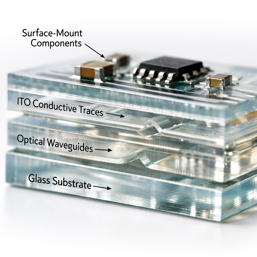
At their core, OPCBs differ fundamentally from traditional flexible or rigid PCBs. The structure typically consists of transparent substrates—often glass, specialized polyimide films, or polyester materials—combined with transparent conductive traces made from materials like indium tin oxide (ITO) or silver nanowires. Unlike conventional copper traces that block light entirely, these conductive pathways maintain optical clarity while routing electrical signals.
The substrate selection drives much of the board’s performance characteristics. Glass substrates offer exceptional transparency, often exceeding 90%, and provide excellent dimensional stability. However, glass lacks the flexibility required for wearable applications and introduces brittleness concerns. Transparent polyimide films present an alternative, combining flexibility with reasonable optical performance, but they introduce thermal expansion challenges and typically achieve lower transparency levels—often in the 70-85% range.
Optical waveguides represent another critical component in OPCB architecture. These structures guide light through specific pathways within the board, enabling optical signal transmission alongside electrical routing. Creating these waveguides requires precise control over material refractive indices and extremely tight manufacturing tolerances. A deviation of just a few microns can significantly degrade optical performance.
The challenge intensifies when these boards must support surface-mount components. Traditional component assembly processes—reflow soldering, for instance—generate temperatures that can damage transparent substrates or degrade their optical properties. This fundamental incompatibility between standard manufacturing processes and transparent materials creates the first major hurdle for mass production.
Current Manufacturing Challenges
The manufacturing obstacles facing AR glasses and medical wearables stem from multiple interconnected factors. Material and process compatibility issues dominate the conversation among design engineers. Transparent substrates, particularly polyimide variants, exhibit extreme temperature sensitivity. Standard reflow profiles reaching 260°C for lead-free soldering can cause yellowing, warping, or complete optical degradation in transparent materials. This forces manufacturers into low-temperature assembly processes that may compromise solder joint reliability or require specialized adhesive bonding techniques that lack established long-term reliability data.
Bonding difficulties compound these thermal concerns. The interface between transparent conductive traces and traditional component terminations presents unique challenges. ITO traces, while optically clear, demonstrate poor adhesion to many common adhesive materials used in flex PCB assembly. Silver nanowire networks, though more flexible than ITO, require protective encapsulation layers that can introduce optical distortions. Each additional layer needed to protect or enhance adhesion reduces overall transparency—creating a design trade-off where improved manufacturability directly compromises optical performance.
Optical losses emerge as another critical concern. Even minor manufacturing variations introduce light scattering, reflection losses, or absorption that degrades system performance. For AR glasses, where every percentage point of transparency affects user experience and battery life, these losses prove unacceptable. Medical wearables face similar constraints when optical sensors must detect subtle biological signals through the transparent substrate. The problem intensifies in multilayer constructions, where each interface between materials creates another opportunity for optical loss.
Mechanical robustness presents paradoxes that challenge traditional PCB engineering wisdom. Transparent substrates must be thin enough to maintain optical clarity and flexibility—often below 100 microns—yet robust enough to withstand repeated flexing, environmental exposure, and mechanical stress from component mounting. Glass substrates achieve excellent optical performance but crack under stress. Flexible transparent films tolerate bending but suffer from creep, dimensional changes with humidity, and vulnerability to chemical exposure.
Consider the specific case of AR glasses. The transparent circuit board must route signals from processing units to micro-displays while flexing around the frame geometry. It must survive daily wear cycles—users putting on and removing glasses, adjusting temple arms, cleaning lenses—while maintaining optical clarity directly in the user’s field of view. Any yellowing, hazing, or mechanical deformation becomes immediately visible and unacceptable. This combination of optical, electrical, and mechanical requirements creates specifications that strain current manufacturing capabilities.
Medical wearables face equally stringent demands but with different emphasis. A transparent wearable sensor monitoring vital signs must maintain optical clarity for sensor accuracy while conforming to body contours, surviving sterilization cycles, and meeting biocompatibility requirements. The transparent substrate must allow light from LEDs to reach the skin and return to photodetectors without significant loss—a requirement that becomes dramatically more challenging when accounting for manufacturing variations across thousands or millions of units.
Scalability and standardization hurdles fundamentally limit production volume. Unlike conventional flex PCB manufacturing, where industry standards like IPC-6013 provide clear specifications and proven processes, transparent PCB manufacturing lacks mature standardization. Each manufacturer develops proprietary processes, making it difficult to second-source materials or transfer designs between suppliers. This absence of standards increases development costs, extends time-to-market, and introduces supply chain risks that procurement specialists rightly view as unacceptable for volume production.
The testing and quality control infrastructure for transparent PCBs remains underdeveloped. Automated optical inspection systems designed for conventional PCBs struggle to detect defects in transparent substrates. Optical performance testing requires specialized equipment and measurement protocols that aren’t standardized across the industry. This makes it difficult to establish consistent acceptance criteria or compare quality levels between suppliers—a situation that quality assurance teams find deeply problematic.
These manufacturing challenges create a self-reinforcing cycle. Limited production volumes prevent economies of scale that would justify investment in specialized equipment. Without standardized processes, each manufacturer’s learning curve remains steep. The high failure rates in early production runs increase costs, which in turn limit market adoption and volume growth. This cycle has persisted for over a decade despite significant investment in transparent electronics research.
Potential Solutions and Future Directions
The path forward requires addressing these challenges through multiple parallel approaches. Silicon photonics integration offers perhaps the most promising long-term solution. By fabricating optical and electrical circuits on the same silicon substrate using semiconductor manufacturing processes, silicon photonics avoids many material compatibility issues that plague hybrid approaches. These integrated optical circuits achieve extraordinary precision—nanometer-scale features are routine—and benefit from decades of semiconductor manufacturing experience.
Silicon photonics faces its own challenges in wearable applications. Silicon substrates aren’t flexible, requiring creative packaging solutions or integration with flexible interconnects. Cost remains high for low-volume applications, though this improves rapidly as production scales. Despite these limitations, silicon photonics provides a technology roadmap with clear scaling potential backed by massive semiconductor industry investment.
Advancements in flexible transparent PCB materials present more immediately applicable solutions. New generations of transparent polyimide films demonstrate improved thermal tolerance, maintaining optical clarity at temperatures approaching conventional reflow profiles. These materials incorporate nanoparticle additives or modified polymer structures that reduce thermal expansion coefficients and improve dimensional stability. While still not matching glass in optical performance, these next-generation materials significantly narrow the gap while retaining flexibility.
Novel conductive materials offering improved thermal tolerance and adhesion are emerging from materials science research. Copper nanowire networks provide an alternative to silver nanowires with better thermal stability. Transparent conductive polymers, though currently limited in conductivity, show promise for low-current applications. Graphene-based transparent conductors combine exceptional electrical properties with mechanical strength, though manufacturing processes remain expensive and difficult to scale.
Adhesion improvements come through surface treatment innovations rather than entirely new materials. Atmospheric plasma treatments modify transparent substrate surfaces at the molecular level, creating chemical bonding sites that dramatically improve adhesion to conductive traces and encapsulation materials. These treatments add minimal cost and integrate easily into existing manufacturing workflows, making them attractive near-term solutions.
The importance of defining optical wavelength requirements early in the design process cannot be overstated. Many OPCB applications don’t require transparency across the entire visible spectrum. AR displays might operate at specific wavelengths, allowing optimization of materials for those wavelengths rather than attempting broadband transparency. Medical sensors typically monitor at narrow bands in the red or infrared spectrum, where different material options become viable. This wavelength-specific approach significantly expands the available material palette and can improve manufacturability substantially.
Engaging with trusted suppliers early in development becomes critical when working with emerging transparent PCB technology. Unlike conventional flex PCB manufacturing, where design-for-manufacturing guidelines are well established, transparent circuits require close collaboration between designers and manufacturers. At Flex Plus, our two decades of experience in advanced flexible PCB manufacturing provides perspective on which transparent circuit approaches can scale to volume production and which remain laboratory curiosities. We evaluate material supply chains, process compatibility, and yield implications before prototypes enter production, reducing risk and accelerating time-to-market.
Supply chain feasibility assessment must occur during design rather than after. Many promising transparent PCB materials suffer from unstable supply chains—small-scale production, single-source suppliers, or uncertain material availability. For products requiring multi-year production runs, these supply chain risks can prove fatal. Experienced manufacturers maintain relationships with material suppliers and understand which materials offer stable, scalable supply chains suitable for volume production.
The future of transparent PCB manufacturing likely involves hybrid approaches rather than single-technology solutions. Combining silicon photonics for dense optical interconnects with flexible transparent films for user-facing surfaces may provide the best balance of performance, manufacturability, and cost. Three-dimensional integration techniques—stacking different substrate types with specialized interconnects—allow each material to perform its optimal function without compromising system-level requirements.
Standards development will eventually unlock mass production. Industry organizations are beginning to address transparent PCB specifications, though progress remains slow. As production volumes increase and more manufacturers invest in the technology, consensus around testing methods, acceptance criteria, and design guidelines will emerge. This standardization follows rather than leads market development—a pattern we’ve observed throughout PCB manufacturing history.
Practical Takeaways for Industry Professionals
For design engineers developing AR glasses or medical wearables, early assessment of design considerations proves essential. Transparent circuits aren’t simply conventional PCBs made with different materials—they require fundamentally different design approaches. Optical path planning must occur simultaneously with electrical routing. Thermal management strategies must account for restricted material options. Mechanical design must recognize the limited fatigue resistance of transparent substrates.
Procurement specialists should evaluate manufacturing partners based on their willingness to engage early in development and their track record with advanced materials. Questions about material sourcing, process development capabilities, and quality control infrastructure reveal which suppliers can support transparent PCB programs through production ramp rather than simply providing prototypes.
Quality assurance teams need to work with suppliers to establish transparent-circuit-specific testing protocols. Standard electrical testing remains necessary but insufficient. Optical performance metrics, mechanical reliability testing under realistic use conditions, and environmental stability assessment all require specialized procedures. Establishing these testing protocols early prevents expensive surprises during production validation.
The value of innovation and collaboration in advancing OPCB technology to meet mass production needs cannot be overstated. No single company possesses all the necessary expertise—materials scientists, optical engineers, manufacturing process experts, and application specialists must collaborate to transform laboratory demonstrations into production reality. Companies willing to share technical challenges and work cooperatively with manufacturing partners accelerate progress far more effectively than those attempting isolated development.
This collaborative approach aligns with Flex Plus‘s vision of supporting technological advancement while maintaining environmental responsibility. Transparent PCBs, when successfully scaled to mass production, enable more efficient AR displays that reduce power consumption, medical devices that minimize disposable components, and wearable electronics that extend product lifecycles through superior user experience. These environmental benefits justify continued investment despite current manufacturing challenges.
The journey from today’s limited-production transparent circuits to true mass manufacturing will require patience, investment, and systematic problem-solving. The obstacles are real and substantial. But they’re not insurmountable. Similar challenges once faced conventional flex PCB manufacturing—we remember when flexible circuits were exotic specialty items rather than mainstream components. Through methodical advancement of materials, processes, and standards, flexible PCBs became reliable, cost-effective building blocks for modern electronics.
Optical transparent circuit boards are following the same path, just several decades behind. For companies willing to engage with the technology’s current limitations while working toward future capabilities, transparent circuits offer genuine competitive advantages in applications where optical integration provides unique value. The question isn’t whether transparent PCBs will achieve mass production—it’s which companies will position themselves to capitalize on that inevitable transition when standardization and manufacturing maturity finally arrive.