
Have you ever watched a promising long flex PCB design crumble during final testing? Perhaps the traces cracked after just a few dozen flex cycles, or impedance values drifted far from your carefully calculated targets. Maybe your manufacturing partner returned prototypes with misaligned layers or adhesion failures that rendered months of design work unusable. These frustrations aren’t random occurrences—they’re symptoms of specific challenges that plague extended flexible circuit designs.
Long flex PCBs represent one of the most demanding applications in flexible circuit technology. When designs fail, the consequences ripple through entire production schedules, delaying product launches and eroding confidence in flexible circuit solutions. For design engineers, procurement specialists, and quality teams working on high-volume production projects, understanding why these failures occur—and more importantly, how to prevent them—becomes mission-critical.
The stakes are particularly high in industries where reliability isn’t negotiable. Automotive electronics operating in harsh thermal environments, medical devices requiring ISO 13485 compliance, and telecommunications infrastructure components all depend on long flex PCBs that must perform flawlessly across thousands or millions of flex cycles. When these circuits fail, the impact extends beyond engineering headaches to affect patient safety, vehicle reliability, and network performance.
Understanding Long Flex PCBs: More Than Just Extended Circuits
Long flex PCBs aren’t simply standard flexible circuits stretched to greater lengths. These specialized designs typically extend beyond 500mm and can reach lengths of 1.6 meters in standard applications, with specialized manufacturing capabilities pushing to 3-4 meters for specific industrial applications. This extended format fundamentally changes how the circuit behaves mechanically, electrically, and thermally.
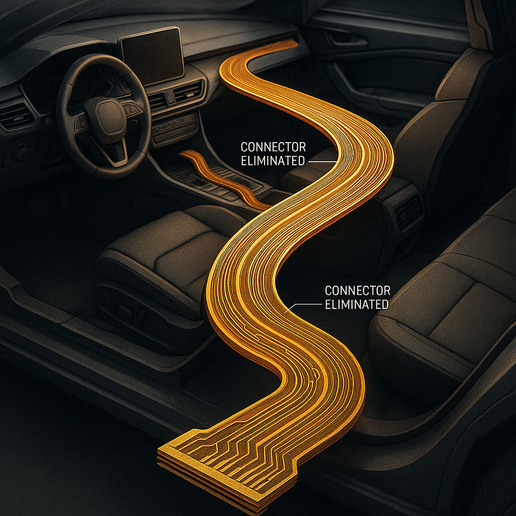
In automotive electronics, long flex PCBs snake through vehicle interiors, connecting dashboard systems to rear compartment electronics while accommodating the complex three-dimensional geometry of modern vehicle architecture. Electric vehicles particularly benefit from these extended circuits, which reduce the weight of traditional wire harnesses by up to 60% while eliminating dozens of connector points that represent potential failure modes. A single long flex PCB can replace what would otherwise require multiple rigid boards connected by fragile wire assemblies.
Medical device manufacturers leverage long flex PCBs to create minimally invasive surgical instruments and patient monitoring systems where space constraints make traditional interconnection methods impractical. The ability to route signals through tight anatomical pathways or around equipment housings while maintaining signal integrity makes these circuits indispensable. Similarly, telecommunications equipment manufacturers use extended flexible circuits in optical transceiver modules and network infrastructure components where high-speed signal transmission must occur across physically separated subsystems.
The value proposition extends beyond simple space savings. Long flex PCBs eliminate mechanical connectors, which in high-reliability applications represent the weakest links in the signal chain. Each connector introduces contact resistance variability, potential corrosion points, and mechanical failure modes. By replacing connector assemblies with continuous flexible circuits, manufacturers can achieve 87% fewer interconnection points—a dramatic improvement in system-level reliability that directly translates to reduced warranty claims and field failures.
Core Design Concepts That Determine Success or Failure
The technical complexity of long flex PCB design centers on managing mechanical stress, maintaining signal integrity, and ensuring manufacturability across extended distances. These challenges interconnect in ways that make isolated solutions ineffective—success requires understanding how design decisions cascade through the entire system.
Bend radius management forms the foundation of reliable long flex PCB design. The fundamental rule states that minimum bend radius should equal at least ten times the total thickness of the flex section. For a typical two-layer design with 25-micron polyimide substrate and 35-micron copper, this translates to roughly 1mm minimum bend radius. However, this simplified rule obscures important nuances. Dynamic flexing applications—where the circuit repeatedly bends and straightens—require more generous bend radii than static applications where the circuit bends once during installation and remains in that configuration.
Consider an automotive application where a long flex PCB routes from the dashboard through the door hinge area to control mirrors and window motors. This circuit experiences thousands of flex cycles as the door opens and closes throughout the vehicle’s lifetime. Engineers must design for a bend radius of 15-20 times the circuit thickness to ensure the copper traces don’t develop fatigue cracks. In contrast, a medical device where the flex circuit wraps around a stationary component during assembly can use the minimum 10x ratio since no dynamic flexing occurs.
Stiffener placement becomes increasingly critical as circuit length increases. Stiffeners are rigid sections—typically FR-4 or polyimide—bonded to specific areas of the flexible circuit to provide mechanical support for components, connector attachment points, or areas requiring dimensional stability. The transition zones between flexible sections and stiffeners represent critical failure points where stress concentrations can cause delamination or copper cracking.
Best practice dictates that stiffener edges should be radiused or chamfered rather than square-cut, and the transition between stiffened and flexible sections should occur over a gradual distance rather than an abrupt change. Many failed designs share a common characteristic: stiffeners extending too close to bend areas, creating stress risers that concentrate mechanical forces at the stiffener edge. Maintaining at least 5mm clearance between stiffener edges and the beginning of bend radii helps distribute stress more evenly.
Rigid-flex transitions in hybrid designs introduce additional complexity. When a long flexible section connects rigid boards at either end, the transition zone requires careful layer stack-up planning. The rigid sections typically use FR-4 with thicker copper weights (70-micron or 2oz), while the flexible sections use thinner polyimide substrates with lighter copper (35-micron or 1oz) to maintain flexibility. The transition must accommodate this change in material thickness and mechanical properties without creating impedance discontinuities or weak mechanical joints.
Layer stack-up architecture profoundly affects both signal integrity and mechanical reliability in extended designs. Single-layer flex circuits offer maximum flexibility and minimum thickness but provide no inherent shielding from electromagnetic interference. Two-layer designs with ground and signal planes significantly improve signal integrity but reduce flexibility and increase minimum bend radius. Multilayer designs of 4-6 layers enable complex routing and excellent signal performance but require careful attention to neutral axis positioning to prevent stress-induced failures.
The neutral axis concept proves essential for multilayer long flex PCBs. When a circuit bends, the outer layers experience tensile stress while inner layers experience compressive stress. The neutral axis—the theoretical plane within the stack-up experiencing zero stress—should ideally align with the copper layers carrying critical signals. Symmetric stack-ups naturally place the neutral axis at the geometric center, but asymmetric designs require careful balancing of layer thicknesses to position the neutral axis optimally.
Routing strategies for long flex circuits deviate from standard rigid PCB conventions. Sharp corners and 90-degree angle traces concentrate stress and create potential crack initiation points. Instead, traces should follow curved paths with radiused corners. The classic “curved teardrop” shape at via connections helps distribute stress where the copper transitions from horizontal to vertical direction. Trace width consistency matters more in flex designs than rigid PCBs because width variations create stress concentration zones where fatigue failures initiate.
Crosshatch or mesh patterns for ground planes rather than solid copper pours significantly improve flexibility while maintaining adequate EMI shielding. Solid copper planes resist bending and can crack under repeated flex cycles. A well-designed mesh pattern with 50-60% copper coverage provides effective shielding while allowing the substrate to flex freely. The mesh pattern should align perpendicular to the expected bend direction to minimize stress on individual copper elements.
Material selection extends beyond the basic choice between polyimide and FR-4. Different polyimide formulations offer varying trade-offs between flexibility, thermal stability, and cost. Standard polyimide performs well to 150°C, while high-temperature formulations maintain properties to 200°C or higher—essential for automotive under-hood applications or industrial process control. Adhesive selection matters equally; acrylic adhesives offer good general-purpose performance, while modified epoxy adhesives provide superior thermal stability and chemical resistance for demanding environments.
Manufacturing Challenges That Derail Long Flex PCB Projects
Even perfectly designed long flex circuits encounter failure modes during manufacturing that shorter circuits easily tolerate. The extended dimensions amplify every process variation, turning minor inconsistencies into yield-killing defects.
Material availability and cost create the first hurdle. While standard flex laminates in 12×18 inch panel sizes readily stock at most manufacturers, long-format materials require special ordering with extended lead times. A 1.5-meter long flex PCB cannot be manufactured from standard panel stock—it requires either roll-to-roll processing or special large-format panels. This constraint immediately narrows the field of capable manufacturers and extends lead times from the typical 1-2 weeks to 3-4 weeks or longer.
Roll-to-roll processing offers advantages for high-volume long flex production but introduces its own challenges. The continuous web of flexible substrate must maintain precise registration as it moves through multiple process steps—imaging, etching, drilling, and final cutting. Any slight drift in registration accumulates across the length of the circuit, potentially causing layer misalignment that renders the board unusable. Our experience across 20+ years of flexible PCB manufacturing has shown that registration control becomes exponentially more difficult as circuit length exceeds one meter.
Registration issues manifest in multiple ways. Layer-to-layer misalignment in multilayer designs can cause internal vias to miss their target pads, creating open circuits. Cover layer misalignment exposes copper traces that should remain protected or covers pads that require soldering. Drill pattern registration errors cause plated through-holes to break through copper pads rather than centering properly. While acceptable registration tolerances for standard circuits measure ±0.075mm, long flex circuits often require tighter tolerances of ±0.05mm or better to maintain yield.
Adhesion problems between layers intensify with length because the larger surface area provides more opportunity for contamination or incomplete bonding. Delamination typically occurs at the interface between polyimide base material and the adhesive layer, or between adhesive and copper foil. Several factors contribute: inadequate surface preparation before lamination, contamination from handling or environmental particles, insufficient lamination pressure or temperature, or incompatible material selections.
Long flex circuits amplify adhesion challenges because the extended length requires longer times in process equipment. If lamination press platens don’t maintain uniform temperature across their entire surface, the edges of a long circuit may receive inadequate heat while the center experiences proper bonding conditions. This variation creates weak adhesion zones that appear functional initially but delaminate during subsequent thermal cycling or mechanical stress.
Fine-line etching across extended lengths requires exceptional process control. Chemical etchants must maintain consistent activity as they flow across the circuit surface. In standard circuits measuring 100-200mm, etchant concentration remains relatively stable. For a 1.5-meter circuit, etchant concentration can vary significantly from entry to exit point, causing over-etching at one end and under-etching at the other. This variation results in trace width inconsistencies that directly impact impedance control and current-carrying capacity.
We’ve developed specialized etching processes that continuously monitor and adjust etchant chemistry across long-format circuits, maintaining trace width tolerances within ±10% even on meter-long designs. This capability distinguishes manufacturers with genuine long flex expertise from those attempting to extend standard processes beyond their reliable operating range.
Thermal management during manufacturing and in application deserves special attention for long flex circuits. Reflow soldering of components generates localized heating that must dissipate through the thin flexible substrate. Unlike rigid PCBs with thick FR-4 cores that conduct heat away from components, flexible circuits provide minimal thermal mass. Long circuits often include sections that bend away from any supporting structure, creating thermally isolated zones where components can overheat during soldering or operation.
Our proprietary thermal management technology integrates flexible heat dissipation channels within the circuit structure, allowing thermal energy to flow along designed pathways rather than concentrating at component locations. This breakthrough addresses the fundamental thermal limitation of extended flexible circuits, enabling higher power components and denser layouts than traditional designs could accommodate.
Proven Design and Manufacturing Best Practices
Successfully producing reliable long flex PCBs requires methodical application of engineering principles validated through real-world production experience. These practices emerged from analyzing thousands of designs across automotive, medical, and telecommunications applications where failure analysis revealed root causes.
Early collaboration with manufacturing partners cannot be overstated. Design for Manufacturing (DFM) analysis should occur during the initial concept phase, not after layout completion. A comprehensive DFMEA (Design Failure Mode and Effects Analysis) identifies potential manufacturing issues before committing to a design direction. This analysis evaluates material availability, process capability limits, registration tolerance requirements, and test strategy feasibility.
In one recent automotive application, early collaboration revealed that the specified 0.05mm trace width and spacing, while theoretically within our fine-line etching capability, would create yield issues at the required 1.8-meter circuit length. By adjusting the design to 0.075mm features during the concept phase, we maintained signal integrity requirements while dramatically improving manufacturing yield from projected 65% to actual 92%. This modification cost nothing to implement early but would have required expensive redesign if discovered during prototype fabrication.
Detailed bend radius specifications must appear on assembly drawings, not just design files. Manufacturing technicians and assembly operators need clear guidance about which areas can flex, minimum allowable bend radii for each zone, and whether bends are static or dynamic. Color-coded zone maps help communicate this information effectively: green zones allow unrestricted handling, yellow zones permit large-radius bends, red zones require stiff support and cannot bend.
Dynamic bend zones should include flex cycle specifications. A circuit designed for 100 flex cycles requires different construction than one requiring 10,000 cycles, even if the bend radius appears identical. For high-cycle applications, we recommend adhesiveless flex constructions where copper is directly bonded to polyimide without intermediate adhesive layers. This eliminates the adhesive as a potential failure mode and significantly extends flex life. Our ultra-thin flex technology, achieving 25-micron total thickness with gold plating on double-sided circuits, enables designs that maintain flexibility through 50,000+ flex cycles in properly designed bend zones.
Robust impedance planning starts with realistic tolerance assumptions. Standard impedance control on rigid PCBs achieves ±10% of target values. Long flex circuits, especially those with multiple bend zones and varying copper weights, require more generous tolerances unless specialized manufacturing processes control the variables. A 50-ohm controlled impedance specification should realistically target ±15% for designs over one meter unless you’re working with a manufacturer offering tighter process control.
Impedance testing strategies for long circuits differ from standard approaches. Rather than testing a single coupon representing the entire design, long flex circuits benefit from multiple test points along the length to verify consistency. We implement distributed test coupons at 300mm intervals on meter-long designs, allowing verification that impedance remains within specification throughout the circuit’s length despite material variations or process drift.
Comprehensive testing protocols must account for the specific failure modes long flex circuits experience. Beyond standard electrical continuity and isolation testing, long flex designs require:
- Flex cycle testing for dynamic bend zones, typically 2-3x the specified operational cycles
- Thermal cycling from -40°C to +125°C to verify adhesion integrity through expansion/contraction cycles
- High-pot testing at elevated voltages to confirm insulation resistance across extended trace lengths
- Visual inspection under magnification at all stiffener transitions and bend zones
- Pull testing of connectors and components to verify adhesion strength
Our testing protocols, developed through IATF 16949 and ISO 13485 certified processes, catch potential reliability issues before circuits reach final assembly. This systematic approach reduced field failures in one medical device application from 2.1% to 0.03%—a 70x improvement that directly resulted from implementing comprehensive testing for a 1.2-meter flex circuit assembly.
Quick Design Checklist for Long Flex PCB Success
Before finalizing your extended circuit design, verify these critical elements:
Bend radii verification: Confirm all specified bend radii meet minimum requirements of 10x total thickness for static bends, 15-20x for dynamic applications. Check that no copper features or vias appear within 2mm of bend zone centerlines.
Stiffener placement review: Verify 5mm minimum clearance between stiffener edges and bend zone beginnings. Confirm all stiffener edges include radius or chamfer specifications. Check that component keepout zones around stiffeners prevent assembly issues.
Transition zone smoothness: Examine all rigid-to-flex transitions for gradual layer stack-up changes. Verify impedance calculations account for material property changes in transition zones. Confirm mechanical support exists for areas immediately adjacent to transitions.
Consistent impedance maintenance: Review trace width consistency throughout the circuit length. Verify ground plane mesh patterns provide adequate coverage without restricting flexibility. Confirm impedance test coupon placement at multiple locations for validation.
Thorough verification processes: Schedule DFM review with your manufacturing partner before ordering prototypes. Plan comprehensive testing including flex cycle, thermal shock, and high-voltage isolation. Document acceptance criteria for visual inspection of critical zones.
The difference between successful long flex PCB designs and failed attempts ultimately comes down to aligning design intent with manufacturing capabilities. Extended flexible circuits push the boundaries of both design engineering and manufacturing process control. By understanding the specific challenges these circuits face—registration control across extended lengths, adhesion integrity with large surface areas, thermal management in thin substrates, and mechanical reliability through thousands of flex cycles—you can make informed decisions that prevent failures before they occur.
At Flex Plus, our 20+ years specializing in flexible and rigid-flex PCB manufacturing has taught us that long circuit success requires more than just extended dimensions—it demands a systematic engineering approach backed by proven manufacturing processes. Our state-of-the-art 16,000+ square meter facility maintains full in-house control from raw material to final testing, enabling the consistent quality extended circuits require. Whether your application demands standard lengths to 1.6 meters or specialized designs reaching 3-4 meters, the foundation remains the same: rigorous design practices, validated manufacturing processes, and comprehensive testing protocols that catch issues before they impact your production schedule.
Your next long flex PCB doesn’t have to fail. With proper design attention to mechanical stress management, careful material selection, realistic tolerance planning, and partnership with a manufacturer who understands the unique challenges of extended flexible circuits, you can achieve the reliability your application demands. The key is recognizing that long flex PCBs aren’t simply stretched versions of standard designs—they’re specialized engineering solutions requiring specialized expertise to manufacture successfully.