
- Understanding Thermal Resistance Networks in Flexible Circuits
- Material Choices That Make or Break Thermal Performance
- Strategic Thermal Management Through Via Design
- Mechanical Heat Sinking in Flexible Assemblies
- Layout Guidelines and Simulation Testing
- Material and Stiffness Considerations in Production Context
- Validation Practices: From Simulation to Reality
- Common Pitfalls and How to Avoid Them
- Conclusion: Integrating Thermal Excellence Into Your Design Process
When your flexible PCB fails thermal testing at the prototype stage, it’s frustrating. When it fails during volume production, it’s catastrophic. Yet thermal management remains one of the most underestimated challenges in high-power flex PCB design, particularly as engineers transition from low-volume prototypes to mass manufacturing.
The consequences are real. An automotive sensor manufacturer recently discovered their flex PCB design—which performed flawlessly in prototype quantities—experienced 18% field failures when scaled to production volumes. The culprit? Inadequate thermal planning that didn’t account for cumulative heat effects in densely packed production assemblies.
This article reveals five critical heat dissipation strategies that even experienced engineers frequently overlook when designing high-power flex PCBs for volume production. These insights come from over 20 years of manufacturing flexible circuits for industries where thermal failure isn’t an option—from electric vehicles to medical devices.
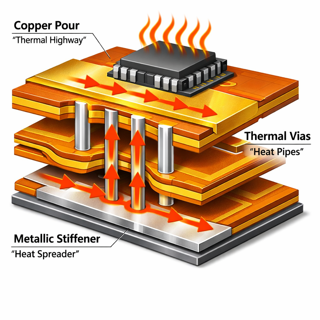
Understanding Thermal Resistance Networks in Flexible Circuits
Before diving into specific strategies, let’s establish a fundamental concept: thermal resistance networks. Unlike rigid PCBs where heat spreads relatively uniformly across FR-4 substrates, flexible circuits create complex thermal pathways that behave differently under various conditions.
Think of heat flow in a flex PCB as water flowing through a network of pipes with different diameters. The thermal resistance is analogous to pipe diameter—narrow pipes (high resistance) restrict flow, while wide pipes (low resistance) allow heat to move freely. In flexible circuits, this network consists of three primary conduction paths:
Copper pours serve as the superhighways of heat dissipation. A 2-ounce copper layer conducts heat approximately 1000 times better than polyimide substrate material. This dramatic difference means that your copper geometry determines roughly 90% of your thermal performance. Engineers who treat copper pours as afterthoughts rather than deliberate thermal design elements inevitably face problems in production.
Thermal vias create vertical heat channels through multilayer structures. Each via acts as a miniature heat pipe, transferring thermal energy from hot components to cooler layers or external heat sinks. The effectiveness of a via depends on three factors: diameter, copper plating thickness, and spacing. A common mistake? Using the minimum via size permitted by your manufacturer’s capabilities rather than the optimal size for thermal transfer.
Stiffeners in flexible PCBs serve dual purposes—mechanical reinforcement and thermal management. When designed correctly, aluminum or copper stiffeners function as integrated heat spreaders, drawing heat away from critical components. A recent project for an industrial control system demonstrated this principle: by repositioning copper stiffeners from purely structural locations to thermally strategic positions, we reduced operating temperatures by 22°C without adding cost.
The challenge in volume production is that these thermal pathways must remain consistent across thousands of units. Small variations in copper thickness, via plating quality, or stiffener bonding that seem insignificant in prototypes become statistically significant failure modes in high-volume manufacturing.
Material Choices That Make or Break Thermal Performance
Material selection for high-power flex PCBs involves complex tradeoffs that aren’t always obvious from datasheets. Let’s examine the thermal implications of common material choices.
Polyimide substrate remains the gold standard for flexible circuits, but not all polyimides perform equally in thermal applications. Standard polyimide exhibits thermal conductivity around 0.12 W/mK—roughly 3000 times lower than copper. This massive disparity means that substrate thickness directly impacts thermal resistance. A 50-micron polyimide layer creates significantly less thermal resistance than a 125-micron layer, yet many engineers default to thicker substrates without considering thermal implications.
For applications requiring extreme thermal performance, some designers specify thermally enhanced polyimides with ceramic fillers that increase thermal conductivity by 200-300%. However, these materials introduce new challenges: reduced flexibility, higher costs, and potential manufacturing complications in volume production.
Adhesive systems create hidden thermal barriers that engineers frequently overlook. Traditional acrylic adhesives used to bond copper to polyimide typically exhibit thermal conductivity below 0.2 W/mK. In a multilayer flex PCB, these adhesive layers accumulate, creating significant thermal resistance through the z-axis. An eight-layer flexible PCB might contain seven adhesive interfaces, each adding thermal resistance.
Adhesiveless constructions eliminate these barriers but require advanced manufacturing capabilities. At FlexPlus, we’ve developed processes for adhesiveless multilayer flex PCBs that reduce through-thickness thermal resistance by up to 40% compared to conventional constructions—a critical advantage for high-power applications requiring efficient heat transfer to external heat sinks.
Metal stiffeners deserve special attention in thermal design. Aluminum stiffeners offer decent thermal conductivity (approximately 205 W/mK) at low weight, making them suitable for applications where weight matters. Copper stiffeners provide superior thermal performance (around 385 W/mK) but add significant mass. The decision between these options should be driven by thermal modeling, not arbitrary cost minimization.
One automotive electronics manufacturer learned this lesson the hard way. Their cost-reduction initiative replaced copper stiffeners with aluminum equivalents without thermal reanalysis. The result: component operating temperatures increased by 15°C, pushing several ICs beyond their maximum junction temperature specifications during worst-case environmental conditions. The subsequent redesign and re-qualification cost exceeded their planned material savings by a factor of eight.
Strategic Thermal Management Through Via Design
Via design for thermal management differs fundamentally from via design for electrical connectivity. Yet many engineers apply electrical design rules to thermal vias, resulting in inadequate heat dissipation.
Via sizing principles for thermal applications start with understanding heat transfer physics. The thermal resistance of a cylindrical via is inversely proportional to its cross-sectional area. Doubling the via diameter reduces thermal resistance by approximately 75%—a dramatic improvement. However, larger vias consume more board area and may create challenges in high-density layouts.
The optimal approach uses thermal modeling to determine minimum effective via diameters for specific heat loads. As a general guideline, thermal vias for components dissipating more than 1 watt should be at least 0.6mm in diameter with minimum 1-ounce copper plating. For components above 3 watts, consider 0.8mm or larger vias.
Via patterns matter as much as individual via size. A single via underneath a high-power component creates a thermal bottleneck. Instead, arrays of vias distribute heat more effectively. Research shows that four 0.6mm vias spaced 1.2mm apart provide better thermal performance than one 1.2mm via, despite having similar total copper cross-section.
The spacing between thermal vias involves counterintuitive physics. Vias placed too close together experience thermal interference—their heat transfer zones overlap, reducing overall effectiveness. Optimal spacing typically ranges from 1.5 to 2 times the via diameter. For 0.6mm vias, this translates to approximately 1mm spacing center-to-center.
Via-in-pad technology offers the most direct thermal path from components to internal copper layers or external heat sinks. This technique places vias directly underneath component pads, eliminating the thermal resistance of traces between pads and vias. However, via-in-pad requires careful manufacturing control to prevent solder wicking through the via during assembly, which can create weak solder joints.
At FlexPlus, we address this challenge through copper-filled via-in-pad processes, where vias are completely filled with copper and planarized. This provides superior thermal performance while ensuring reliable solder joints—critical for high-volume production where assembly consistency determines yield.
Mechanical Heat Sinking in Flexible Assemblies
One of the most overlooked strategies in high-power flex PCB design is the integration of mechanical heat sinking directly into the flexible assembly. Unlike rigid PCBs where heat sinks can be easily mounted with standard hardware, flexible circuits require creative approaches to thermal extraction.
Bonded heat spreaders represent the most common mechanical thermal management solution for flex PCBs. These are typically thin metal plates—aluminum or copper—adhered to the flexible circuit using thermally conductive adhesives. The effectiveness of this approach depends critically on adhesive selection and bonding process control.
Thermally conductive adhesives vary widely in performance, as explained in thermal management best practices for power conversion circuits. Standard adhesives might exhibit thermal conductivity around 1 W/mK, while high-performance formulations reach 3-5 W/mK. This difference matters: a 100-square-millimeter bonded copper spreader with 1 W/mK adhesive creates roughly 3 times the thermal resistance compared to the same spreader with 4 W/mK adhesive.
Process control in adhesive application becomes critical in volume production. Inconsistent adhesive thickness creates thermal performance variability across production lots. We’ve seen cases where adhesive thickness variations of just 50 microns resulted in 8°C temperature differences between samples—enough to cause intermittent failures in margin-limited designs.
Integrated stiffeners with thermal function provide an elegant solution that kills two birds with one stone. By positioning copper or aluminum stiffeners directly beneath high-power components, you gain both mechanical support and thermal management without adding assembly steps. However, this requires tight coordination between electrical and mechanical design teams—something that often breaks down in larger organizations.
A medical device manufacturer we worked with discovered this integration opportunity during design optimization. Their initial design used separate stiffeners for mechanical support and bonded heat spreaders for thermal management. By redesigning stiffener locations to align with thermal hotspots and increasing stiffener thickness from 0.3mm to 0.5mm copper, they eliminated the need for separate heat spreaders entirely. This simplification reduced assembly cost by 12% while actually improving thermal performance.
Passive versus active cooling decisions significantly impact design strategy. Passive cooling relies solely on conduction and natural convection—heat flows from components through the PCB structure to the ambient environment. Active cooling introduces forced airflow or liquid cooling to enhance heat transfer rates.
Most high-power flex PCB applications in electric vehicles, industrial controls, and telecommunications equipment operate in environments with some level of airflow—either from cooling fans or natural convection within enclosures. Designing to leverage this airflow requires careful component placement and thermal pathway planning. Position high-power components where they can benefit from airflow, and ensure thermal pathways lead to external surfaces where convection can occur.
Layout Guidelines and Simulation Testing
Theoretical thermal design means nothing without practical implementation through layout and verification through testing. Here are specific guidelines that translate thermal strategy into manufacturable designs.
Component spacing rules for high-power flex PCBs differ from standard spacing guidelines. While electrical clearance might permit placing components 1mm apart, thermal considerations often require 3-5mm minimum spacing between power components to prevent thermal coupling. When two components operating at 80°C are placed too close together, the local ambient temperature between them rises above 90°C, pushing both components beyond their thermal limits even though neither alone would overheat.
Our rule of thumb: maintain minimum spacing equal to the largest component dimension between high-power devices. For a 5mm × 5mm power IC, keep at least 5mm clearance to adjacent heat-generating components. This guideline, derived from countless thermal simulations and real-world measurements, prevents the majority of thermal coupling issues.
Copper thickness optimization involves balancing thermal performance, flexibility, and cost. Thicker copper provides better thermal conductivity but reduces flexibility and increases material cost. For high-power applications, 2-ounce copper (70 microns) typically represents the sweet spot—sufficient thermal performance without completely sacrificing flexibility. Some applications require even thicker copper in localized areas, achievable through stepped copper thickness designs.
One industrial sensor application demonstrates this principle. The design required 3-ounce copper beneath a high-current power stage but only 1-ounce copper in signal areas. By using stepped copper construction—3-ounce in power areas transitioning to 1-ounce in flex regions—we achieved thermal performance requirements while maintaining flexibility in bend areas. This hybrid approach costs more than uniform copper thickness but far less than using 3-ounce copper throughout.
Thermal relief patterns deserve mention even though they’re commonly associated with reducing thermal stress during soldering. In high-power flex PCBs, thermal reliefs serve an additional purpose: controlled thermal resistance to prevent excessive heat flow into temperature-sensitive components. A power transistor might operate safely at 100°C, but an adjacent sensor might fail above 70°C. Strategic thermal relief patterns between these components create deliberate thermal isolation.
Thermal simulation tools have become indispensable for high-power flex PCB design. Software packages like ANSYS, Flotherm, or even simpler tools built into modern PCB design suites allow engineers to predict thermal behavior before committing to manufacturing. These simulations reveal hotspots, validate via patterns, and optimize heat sink designs with far greater accuracy than analytical calculations.
However, simulation accuracy depends on accurate material properties and boundary conditions. Garbage in, garbage out—as the saying goes. When setting up thermal simulations, verify your material properties against manufacturer datasheets, account for actual assembly conditions including conformal coatings and enclosure effects, and always validate simulation results against physical measurements on actual prototypes.
At FlexPlus, we’ve developed validated thermal models for our standard material stack-ups and constructions. This library of verified thermal properties allows us to provide rapid thermal feedback during design reviews, often identifying potential issues before the first prototype is built. This Design for Manufacturing (DFM) approach, backed by ISO 9001, ISO 13485, and IATF 16949 certifications, exemplifies how manufacturing expertise should inform design decisions.
Material and Stiffness Considerations in Production Context
The transition from prototype to volume production magnifies the importance of material consistency and stiffness control. Small variations that seem insignificant in single units become statistically relevant across thousands of assemblies.
Aluminum versus copper stiffeners involves more than just thermal conductivity differences. Aluminum’s lower density (2.7 g/cm³ versus copper’s 8.9 g/cm³) makes it attractive for weight-sensitive applications like drones, wearable devices, and portable medical equipment. However, copper’s 88% higher thermal conductivity means you can use a thinner copper stiffener to achieve the same thermal performance as aluminum—partially offsetting the weight difference.
The decision framework should consider thermal requirements first, weight constraints second, and cost third. For applications where thermal performance drives stiffener selection, copper typically wins. For weight-critical applications where thermal requirements are moderate, aluminum makes sense. Never let cost alone determine this choice—the potential field failure costs dwarf material savings.
Bonding adhesive selection for stiffeners affects both thermal and mechanical performance. Thermally conductive adhesives optimize heat transfer but may exhibit lower mechanical strength compared to structural adhesives. Some applications require both properties, necessitating hybrid bonding approaches or adhesive formulations specifically engineered for combined thermal and mechanical performance.
Production consistency in adhesive application determines whether your thermal design performs reliably across all units. Automated adhesive dispensing systems provide far better thickness control than manual application, reducing thermal resistance variations from unit to unit. This consistency matters most in high-volume production where statistical process control becomes essential.
Validation Practices: From Simulation to Reality
Even the most sophisticated thermal design requires validation through physical testing. Simulation predicts behavior under ideal conditions, but reality introduces manufacturing variations, assembly tolerances, and environmental factors that models cannot fully capture.
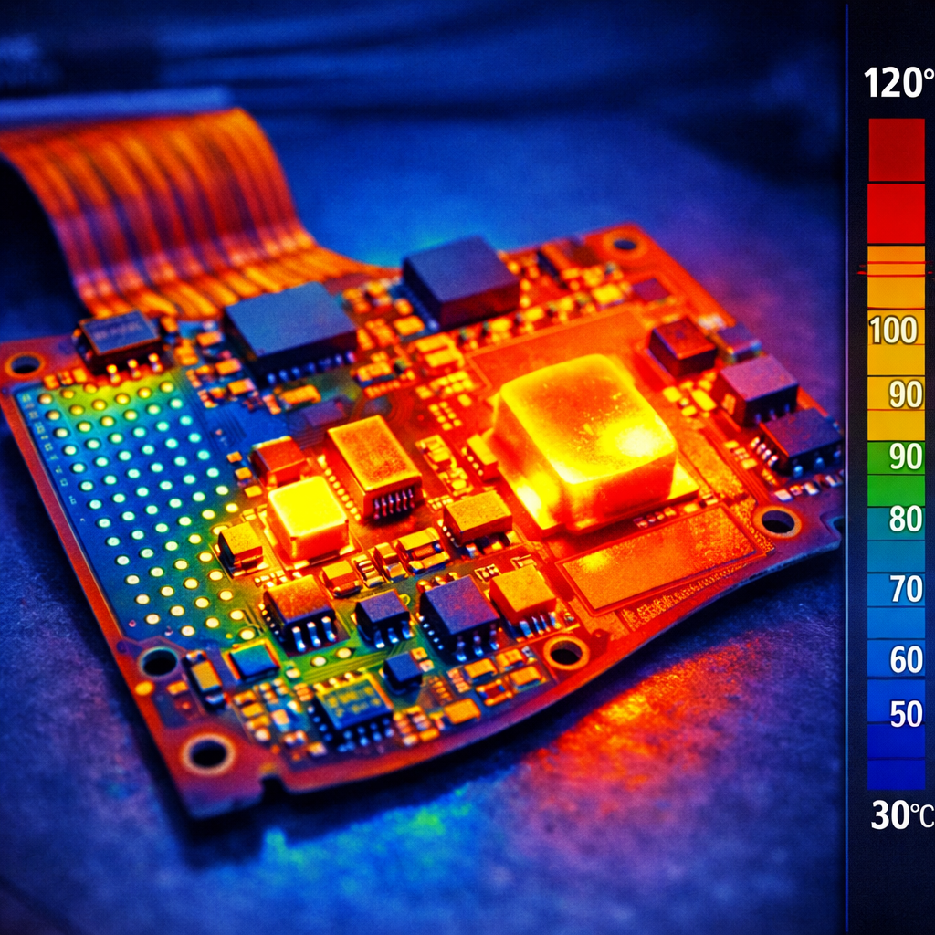
Thermal imaging provides visual verification of heat distribution across your flex PCB assembly. Infrared cameras reveal hotspots, identify areas where heat isn’t flowing as intended, and validate that thermal pathways perform as designed. We recommend thermal imaging on first prototypes under maximum power conditions to verify simulation predictions match reality.
One telecommunications equipment manufacturer used thermal imaging to discover that their bonded heat spreader wasn’t making uniform contact with the underlying flex PCB. Adhesive thickness variations created air gaps in certain areas, drastically reducing thermal performance. This issue—invisible in electrical testing—would have caused random field failures if not caught during prototype validation.
Thermocouple measurements provide quantitative temperature data at specific points. Strategic placement of thermocouples on high-power components, at via locations, and on heat sinks allows you to build a detailed temperature map of your assembly under various operating conditions. This data validates thermal models and establishes temperature margins for reliability assessment.
For volume production validation, we recommend testing at temperature extremes beyond normal operating range—both hot and cold environmental conditions combined with maximum power dissipation. A design that operates acceptably at 25°C ambient but fails at 60°C ambient won’t survive automotive or industrial applications where such temperatures are routine.
Accelerated life testing at elevated temperatures reveals long-term reliability issues before they occur in the field. Operating samples at maximum junction temperatures for extended periods stresses adhesive bonds, solder joints, and material interfaces—identifying potential failure mechanisms. This testing is expensive and time-consuming, but far less costly than product recalls or warranty claims.
At FlexPlus, we’ve established accelerated testing protocols for high-power flex PCB applications based on our 20+ years of manufacturing experience. These protocols, aligned with IATF 16949 automotive standards and ISO 13485 medical device requirements, provide confidence that designs will survive their intended operational lifetime.
Common Pitfalls and How to Avoid Them
Even experienced engineers fall into predictable thermal design traps when designing high-power flex PCBs. Here are the most common failures we’ve observed—and how to prevent them.
Underestimating cumulative effects tops the list. Individual components might each operate within specifications, but their combined heat output raises local ambient temperature throughout the assembly. We’ve seen designs where five components each dissipating 0.5 watts—seemingly modest power levels—created a local temperature rise of 35°C because they were clustered too closely together.
The solution: always analyze thermal performance at the system level, not just component level. Use thermal simulation to model the entire assembly under worst-case conditions: maximum ambient temperature, maximum power dissipation, minimum airflow. Design for these extremes, not typical conditions.
Ignoring manufacturing tolerances creates another common failure mode. Your thermal design might work perfectly with nominal copper thickness, ideal via plating, and perfect stiffener bonding—but what happens when copper thickness varies by ±10%, via plating is at minimum specification, and stiffener adhesive thickness varies by 20%? These manufacturing realities, statistical certainties in volume production, can transform a marginal design into a failure.
Build thermal margin into your design by assuming worst-case manufacturing tolerances. If your thermal model shows a component operating at 118°C with a 125°C maximum rating under nominal conditions, that 7°C margin will evaporate with tolerance stack-up. Target at least 15-20°C margin below maximum ratings to accommodate real-world manufacturing variations.
Neglecting certification requirements causes expensive redesigns in regulated industries. Automotive applications require IATF 16949 certification, medical devices need ISO 13485 compliance, and many applications require UL recognition. These certifications impose specific thermal testing requirements and design constraints that cannot be retrofitted after the design is complete.
Engage with your manufacturing partner early to understand certification requirements. At FlexPlus, our engineering team provides certification guidance during the design phase, helping customers avoid the costly mistakes of designing without considering compliance requirements.
Conclusion: Integrating Thermal Excellence Into Your Design Process
High-power flex PCB heat dissipation isn’t an afterthought to be addressed during prototype troubleshooting—it’s a fundamental design consideration that must be integrated from the earliest concept stages. The five critical strategies we’ve explored—understanding thermal resistance networks, optimizing material choices, strategic via design, mechanical heat sinking integration, and rigorous validation—form a comprehensive framework for thermal excellence.
As you move from prototype to volume production, remember that thermal performance consistency becomes as important as thermal performance itself. Manufacturing variations, tolerance stack-ups, and assembly processes all influence how effectively your design dissipates heat across thousands of units.
Partner with a manufacturer who understands these challenges. At FlexPlus, our 20+ years of specialized flexible PCB manufacturing experience, backed by ISO 9001, ISO 13485, and IATF 16949 certifications, ensures that thermal design strategies translate reliably from prototype to mass production. Our comprehensive Design for Manufacturing (DFM) support identifies potential thermal issues before they become production problems, saving time, cost, and field failure headaches.
The next time you design a high-power flex PCB, treat thermal management with the same rigor you apply to electrical design. Your customers—and your field reliability statistics—will thank you.