
Understanding the flexible PCB manufacturing process isn’t just about satisfying curiosity—it’s about making smarter decisions that impact your product’s reliability, cost, and time-to-market. Whether you’re an R&D engineer designing a next-generation medical device or a procurement specialist evaluating manufacturing partners, knowing what happens between your design file and the finished circuit empowers you to optimize for success.
For industries like automotive electronics, medical devices, and consumer technology, flexible PCBs have become indispensable. They enable form factors impossible with rigid boards, reduce weight in electric vehicles, and provide the reliability required for life-critical medical implants. Yet the path from concept to production-ready circuits involves precision engineering at every stage. Let’s walk through the ten critical steps that transform your design into a flexible circuit capable of meeting stringent industry standards.
Step 1: Design and Layout Creation
Every successful flexible PCB begins with thoughtful design. This stage sets the foundation for manufacturability, reliability, and cost-effectiveness. Engineers use CAD tools to define circuit constraints, optimize trace routing, and plan for the unique mechanical demands of flexible circuits.
Unlike rigid PCBs, flexible designs must account for dynamic bending, twisting, and the stresses these movements create on copper traces. Trace routing follows specific rules—avoiding right angles in bend areas, maintaining adequate spacing for flexibility, and positioning components strategically to prevent stress concentration. Early planning for layer stacking determines how rigid and flexible sections integrate, while stiffener requirements define where additional support prevents excessive bending or provides mounting points.
At Flex Plus, we’ve learned through 20+ years of experience that catching design issues early saves months in production cycles. Our Design for Manufacturing (DFM) support evaluates designs against real-world manufacturing constraints, identifying potential problems before they become expensive mistakes. We’ve seen projects where simple trace rerouting in the design phase prevented yield issues that would have surfaced during mass production.
Step 2: Material Selection
Material selection balances flexibility, durability, thermal performance, and cost. The substrate forms the foundation—polyimide (PI) remains the industry standard for its exceptional heat resistance and mechanical properties, while specialized applications might call for thermoplastic polyurethane (TPU) for biocompatibility or extreme flexibility.
Copper weight matters more than many realize. Thinner copper (18μm or ½ oz) provides better flexibility and tighter bend radii, ideal for dynamic flexing applications like wearable devices. Thicker copper (70μm or 2 oz) carries higher currents but reduces flexibility, making it suitable for power distribution in automotive harnesses. The choice depends on your electrical requirements and mechanical environment.
Adhesives bond layers together, but they introduce trade-offs. Adhesive-based constructions offer lower costs and proven reliability for many applications. Adhesiveless constructions provide superior flexibility and thermal performance, critical when your flexible PCB must survive hundreds of thousands of flex cycles or operate at elevated temperatures.
Environmental factors guide these decisions too. Will your circuit experience temperature cycling from -40°C to 125°C in an automotive application? Does it need to withstand sterilization cycles in a medical device? Our material consultation service helps engineers navigate these choices, selecting substrates and copper weights that meet both electrical specifications and environmental demands.
Step 3: Lamination and Layer Bonding
Lamination transforms separate material layers into an integrated structure. This process demands precision in temperature, pressure, and timing—variables that directly impact dimensional accuracy and layer bonding quality.
The stack-up gets assembled in a clean environment: base substrate, copper foil, adhesive layers (if used), and coverlay materials. This entire stack enters a lamination press where controlled heat activates adhesives and pressure removes air gaps while bonding layers together. Temperature profiles must match material specifications exactly. Too low and adhesives won’t fully cure; too high and polyimide substrates can degrade or dimensional stability suffers.
Pressure distribution across the panel ensures uniform bonding. Uneven pressure creates weak spots that may delaminate under mechanical stress or thermal cycling. Timing matters because different adhesive systems require specific dwell times at target temperatures for optimal cross-linking.
For multilayer flexible PCBs with 3-8 layers, this process repeats with additional cycles, each building upon the previous lamination. Rigid-flex constructions add complexity, bonding rigid FR-4 sections to flexible polyimide layers with specialized no-flow prepregs that prevent resin migration into flex areas where it would compromise flexibility.
Our ISO 9001 and IATF 16949 certifications ensure these critical parameters remain tightly controlled through continuous monitoring and validation, maintaining dimensional accuracy within microns across panels up to 1.6 meters long.
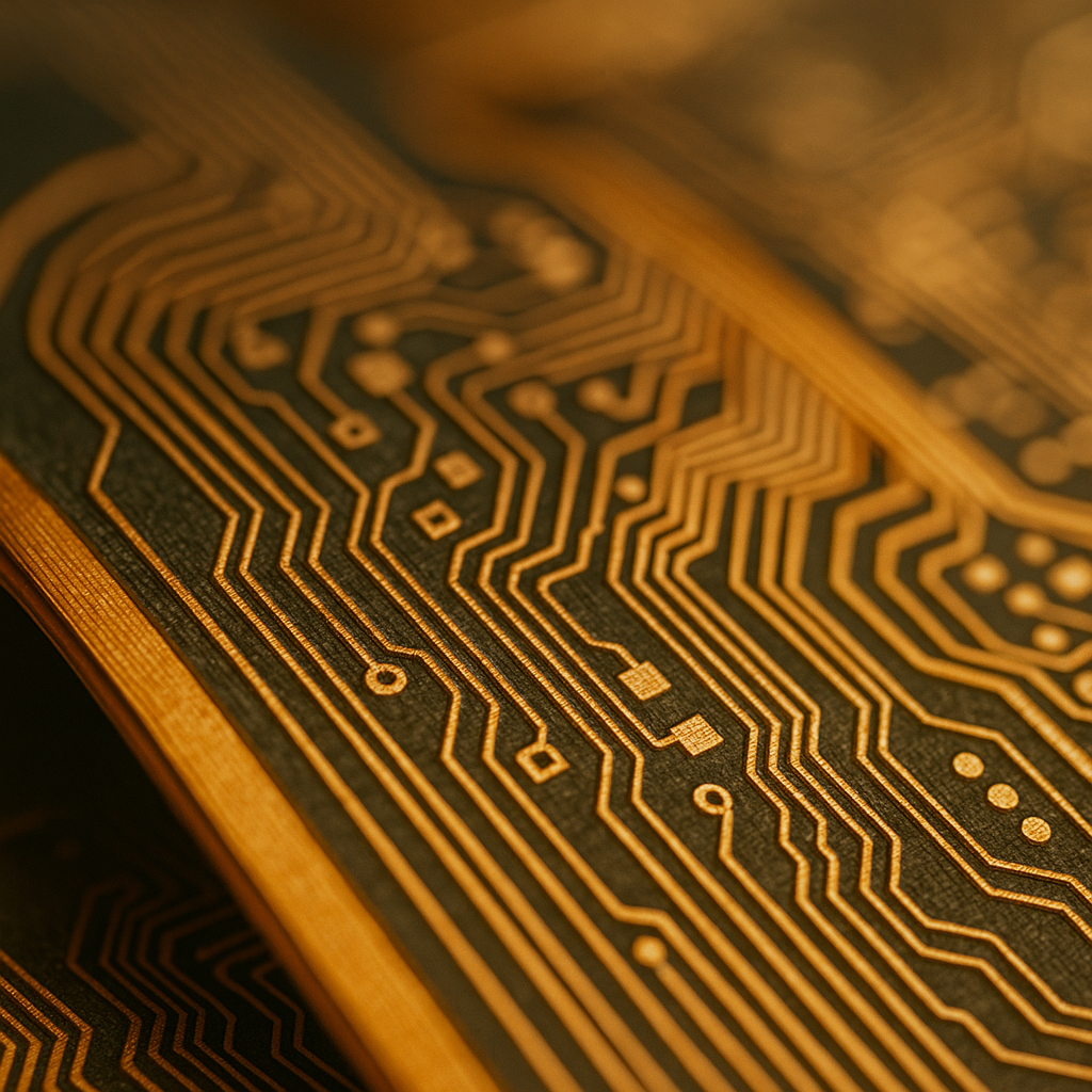
Step 4: Circuit Patterning Through Imaging and Photolithography
Circuit patterning transfers your design onto the copper layers with microscopic precision. This photolithographic process determines whether your fine-pitch traces and tight spacing become reality or manufacturing scrap.
The laminated panel receives a photosensitive resist coating—a light-reactive film that will define your circuit pattern. Your CAD design becomes a photomask, essentially a high-resolution negative of your circuit traces. UV light exposure through this mask selectively hardens or softens the resist, creating a protective pattern over areas that will become traces.
Pattern fidelity becomes critical here, especially for high-density interconnect designs with 0.05mm traces and spaces—designs increasingly common in smartphones and wearables. Alignment accuracy between layers affects via registration, which impacts electrical performance and reliability. Even slight misalignment can create opens or shorts in complex multilayer stackups.
For flexible PCBs, the challenges multiply. Flexible substrates can distort slightly during processing, requiring compensation in imaging and registration. Advanced imaging equipment accounts for these dimensional changes, maintaining pattern accuracy across long panels where thermal expansion alone could shift features by dozens of microns.
Step 5: Etching and Cleaning
Etching removes unwanted copper, leaving only the circuit traces defined during imaging. Chemical etchants dissolve exposed copper with remarkable selectivity, while the resist layer protects your intended circuit pattern.
The etching process must maintain uniformity across the entire panel. Over-etching narrows traces below design specifications, potentially increasing resistance or reducing current-carrying capacity. Under-etching leaves copper residue that can create shorts between adjacent traces. Etch rates vary with copper thickness, panel size, and bath chemistry, requiring continuous monitoring and adjustment.
Edge definition matters particularly for flexible PCBs where traces may be narrower and closer together than rigid board designs. Clean, vertical etch profiles ensure trace widths match design specifications and prevent “undercut” where the etchant erodes beyond the resist edge.
After etching, thorough cleaning removes all resist residue and etching chemistry. Any remaining contaminants can affect subsequent plating steps or cause reliability issues during the circuit’s operational life. Our cleaning processes follow strict protocols validated through ISO 13485 certification, critical for medical device applications where contamination is unacceptable.
Step 6: Drilling and Via Formation
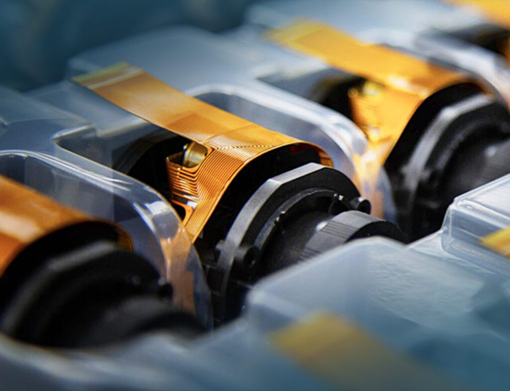
Vias create electrical connections between layers, requiring precision drilling that maintains via quality and registration across all layers. Flexible PCBs use both mechanical drilling and laser ablation, each suited to different via types and sizes.
Mechanical drilling handles larger vias and through-holes, using specialized drill bits optimized for polyimide substrates. Laser drilling excels at microvias—those tiny connections between adjacent layers in HDI designs. Lasers create clean, precise holes without the mechanical stress that drills impose on flexible substrates.
Registration accuracy determines whether vias actually connect the intended layers. Misaligned vias create reliability nightmares—intermittent connections that pass initial testing but fail under thermal cycling or mechanical stress. Our drilling processes maintain registration tolerances within microns, verified through automated optical inspection that checks every via’s position against design specifications.
For rigid-flex PCBs, drilling strategies adapt to mixed materials. Rigid sections with FR-4 substrates drill differently than flexible polyimide sections. Stack drilling multiple layers simultaneously requires parameter optimization that prevents delamination or hole quality issues at layer interfaces.
Step 7: Copper Plating and Surface Finishing
Electroplating deposits additional copper onto traces and within vias, achieving required conductor thickness and ensuring reliable interlayer connections. The plating bath contains copper ions that deposit onto exposed copper surfaces when electrical current flows through the panel.
Plating uniformity challenges increase with panel size and circuit complexity. Areas with dense circuitry can plate differently than sparse regions due to current distribution effects. Our plating processes compensate for these variations, achieving thickness uniformity that meets IPC-6013 standards for flexible circuits.
Surface finishing protects copper from oxidation and provides solderability for component attachment. Several options exist, each with advantages:
Immersion gold (ENIG) offers excellent solderability and extended shelf life, ideal for assemblies that may wait weeks between fabrication and assembly. OSP (Organic Solderability Preservative) provides a cost-effective option for circuits proceeding directly to assembly. Immersion silver balances performance and cost for many applications.
The choice depends on your assembly timeline, environmental exposure, and whether the flexible PCB will undergo multiple reflow cycles during assembly—scenarios we discuss during material consultation to ensure your surface finish matches your assembly process requirements.
Step 8: Coverlay Application and Insulation
Coverlay serves as both electrical insulation and mechanical protection for your flexible circuit. This polyimide film with adhesive backing gets laminated over exposed circuit areas, leaving openings only where components mount or connections occur.
Coverlay windows define solderable areas with precise registration to component pads. Window accuracy affects assembly yield—windows too small obstruct soldering access, while oversized windows reduce insulation and mechanical protection. Our coverlay application processes maintain window tolerances that support automated assembly while maximizing circuit protection.
Insulation resistance testing validates that coverlays adequately insulate traces, particularly critical under dynamic bending where flexing might create pinhole failures or crack insulation. Testing simulates operational bending while measuring insulation resistance, ensuring your circuit maintains electrical integrity throughout its flex life.
For ultra-thin designs—like our specialized double-sided flex PCBs down to 25 microns—coverlay selection becomes even more critical. Thinner coverlays maintain flexibility but require careful handling and application to prevent damage or wrinkles that could compromise insulation.
Step 9: Rigid-Flex Transitions and Structural Integrity
Many flexible PCBs incorporate rigid sections for component mounting or connector interfaces. These rigid-flex transitions require careful engineering to maintain structural integrity under flexing conditions.
Stiffeners—polyimide or FR-4 sections bonded to flexible areas—provide localized rigidity without sacrificing flexibility elsewhere. Stiffener placement follows design intent, supporting components, reducing stress on solder joints, and defining fixed mounting points. Adhesive selection affects both mechanical strength and thermal performance, with considerations for operating temperature ranges and assembly processes.
The transition zones where rigid meets flexible represent potential failure points. Our proprietary thermal pathway technology addresses this challenge, managing heat dissipation through flexible circuits while maintaining mechanical integrity. This proves particularly valuable in high-power LED applications or automotive electronics where thermal management directly impacts reliability.
Validation testing subjects rigid-flex assemblies to mechanical flexing cycles while monitoring electrical continuity and visual inspection for delamination or cracking. Our testing protocols simulate operational conditions, with cycle counts and bend radii matching your application requirements. For automotive applications requiring IATF 16949 certification, this testing follows industry-specific standards ensuring reliability through vehicle life cycles.
Step 10: Final Inspection, Testing, and Preparation for Assembly
Quality assurance brings together visual inspection, automated optical inspection (AOI), and electrical testing to verify every flexible PCB meets specifications before it reaches your assembly line.
Visual inspection catches surface defects, contamination, or damage that automated systems might miss. Our inspectors, trained to IPC standards, examine coverlay adhesion, edge definition, and surface finish quality. AOI systems scan entire panels at microscopic resolution, verifying trace widths, spacing compliance, and absence of copper residue or shorts.
Electrical testing validates circuit functionality. Flying probe testers check continuity, insulation resistance, and impedance without requiring custom fixtures. For volume production, dedicated test fixtures enable faster throughput while maintaining test coverage. Our testing protocols adapt to your requirements, from basic continuity testing to complex impedance verification for high-speed signals.
For customers utilizing our full assembly services, preparation includes confirming component footprints, verifying soldermask or coverlay openings, and coordinating with assembly process requirements. This integrated approach—from flexible PCB manufacturing through complete PCBA—reduces vendor coordination, minimizes quality handoff issues, and accelerates time-to-market.
Our commitment to certified excellence shows throughout this final stage. ISO 13485 certification for medical device applications demands traceability and documentation proving every process step met specifications. IATF 16949 certification for automotive applications requires statistical process control and continuous improvement documentation. These aren’t just certifications hanging on a wall—they represent systematic quality management integrated into every manufacturing step.
Bringing It All Together
The flexible PCB manufacturing process involves far more than simply etching copper on polyimide film. Each step builds upon previous work, with precision requirements that compound through the process. Understanding these steps helps you make informed decisions during design, material selection, and manufacturing partner evaluation.
At Flex Plus, our 20+ years of specialized experience means we’ve refined these processes through thousands of projects across diverse industries—from automotive harnesses stretching 3-4 meters to ultra-thin medical implants measuring 25 microns. Our end-to-end manufacturing control, from raw materials to final inspection, eliminates the quality inconsistencies and communication delays that plague broker relationships.
When you partner with a manufacturer who truly understands the flexible PCB manufacturing process—who can explain how material choices affect your thermal requirements, who maintains process controls certified to international standards, who provides engineering support from design through production—you gain more than a supplier. You gain a partner invested in your product’s success.
Whether you’re developing next-generation wearables, designing electric vehicle battery management systems, or creating life-saving medical devices, the flexible circuits enabling your innovation deserve manufacturing excellence at every step. That’s the commitment we bring to every project, every day, for every customer who trusts us with their designs.