
When an automotive supplier’s new sensor design failed qualification testing three times, the root cause wasn’t the components or the assembly process. The problem traced back to impedance mismatches and inadequate thermal management—issues that originated in the initial PCB design files. After partnering with a professional PCB design service to redesign the layout, the sensor passed certification on the first attempt and entered volume production within weeks.
This scenario illustrates a fundamental truth in electronics manufacturing: the quality of your design files determines whether your product succeeds or struggles through production. Industry research consistently shows that proper PCB design accounts for approximately 60% of manufacturing success, while the remaining 40% depends on fabrication quality and assembly processes. When your design files are manufacturing-ready, production flows smoothly. When they contain hidden flaws, every downstream process suffers.
What Makes a PCB Design Service Truly Professional
A professional PCB design service transforms your product concept into manufacturing-ready files through a comprehensive engineering process. This isn’t simply drawing traces and placing components—it’s a systematic approach that considers electrical performance, mechanical requirements, thermal management, and manufacturability from the first sketch to the final Gerber file.
The process begins with understanding your product requirements. What environment will the device operate in? What certifications does it need? What are the size constraints? A medical device requires different design considerations than an automotive sensor, even if they use similar components. Professional design engineers ask these questions upfront because the answers shape every subsequent decision.
During the concept phase, engineers create block diagrams that map out the system architecture. They select appropriate components, considering not just electrical specifications but also availability, cost, and lifecycle stability. This foundation prevents expensive redesigns later when a critical component becomes obsolete or unavailable—similar to how quick turn PCB services enable rapid design iteration during the prototyping phase. This foundation prevents expensive redesigns later when a critical component becomes obsolete or unavailable.
Schematic capture translates the concept into detailed electrical connections. Professional designers create schematics that are both electrically correct and easy to review, using clear component designators and logical signal grouping. The schematic becomes the blueprint that guides layout design and serves as documentation for future modifications.
The layout phase transforms the schematic into a physical design. This stage demands both technical expertise and practical manufacturing knowledge. Engineers must route high-speed signals to maintain signal integrity, place components to optimize thermal dissipation, and ensure that every trace and pad meets the manufacturer’s capabilities.
Throughout this process, professional design services maintain close communication with clients. Regular design reviews ensure the layout matches expectations before moving to the next phase. This collaborative approach catches misunderstandings early, when changes are simple and inexpensive.
The final manufacturing handoff includes comprehensive documentation: schematics, bills of materials, layout files, and manufacturing data in industry-standard formats. These deliverables contain everything a PCB manufacturer needs to fabricate boards exactly as designed.
Critical Technical Concepts That Determine Manufacturing Success
Several technical concepts separate amateur PCB designs from professional ones. Understanding these concepts—and implementing them correctly—directly impacts whether your boards function reliably in volume production.
Stackup design defines how copper layers, insulation materials, and other elements combine to form the complete board structure. A well-designed stackup provides adequate routing space, controls impedance for high-speed signals, and manages electromagnetic interference. For flexible PCBs, stackup design also determines bending characteristics and mechanical durability. Professional designers select materials and layer arrangements that balance electrical performance with manufacturing feasibility.
Impedance control becomes critical for high-speed digital signals and RF applications. When trace impedance doesn’t match the driver and receiver expectations, signal reflections cause data errors and electromagnetic emissions. Controlled impedance design requires careful consideration of trace geometry, dielectric properties, and manufacturing tolerances. Professional design services calculate trace widths, spacing, and dielectric properties to achieve target impedances like 50 ohms or 100 ohms differential. They also specify impedance tolerance requirements so manufacturers can verify the finished boards meet specifications.
Power integrity ensures that every integrated circuit receives stable, clean power despite rapidly changing current demands. Poor power distribution causes voltage droops, ground bounce, and system instability. Professional designs include adequate decoupling capacitors placed strategically near power pins, wide power traces or planes to minimize resistance, and careful attention to return current paths.
Consider a smartphone camera module that experienced intermittent focus failures. Investigation revealed voltage droops on the motor driver power supply during rapid focus changes. The original design used narrow power traces and had insufficient decoupling capacitance. A professional redesign with proper power distribution planes and optimized capacitor placement eliminated the failures completely.
Thermal management prevents components from overheating during operation. Professional designers analyze power dissipation, select appropriate copper weights to conduct heat away from hot components, and incorporate thermal vias for effective heat management. For flexible PCBs, thermal management becomes more challenging because the substrate has poor thermal conductivity compared to rigid FR-4 boards. Advanced techniques like flexible heat dissipation channels can dramatically improve thermal performance.
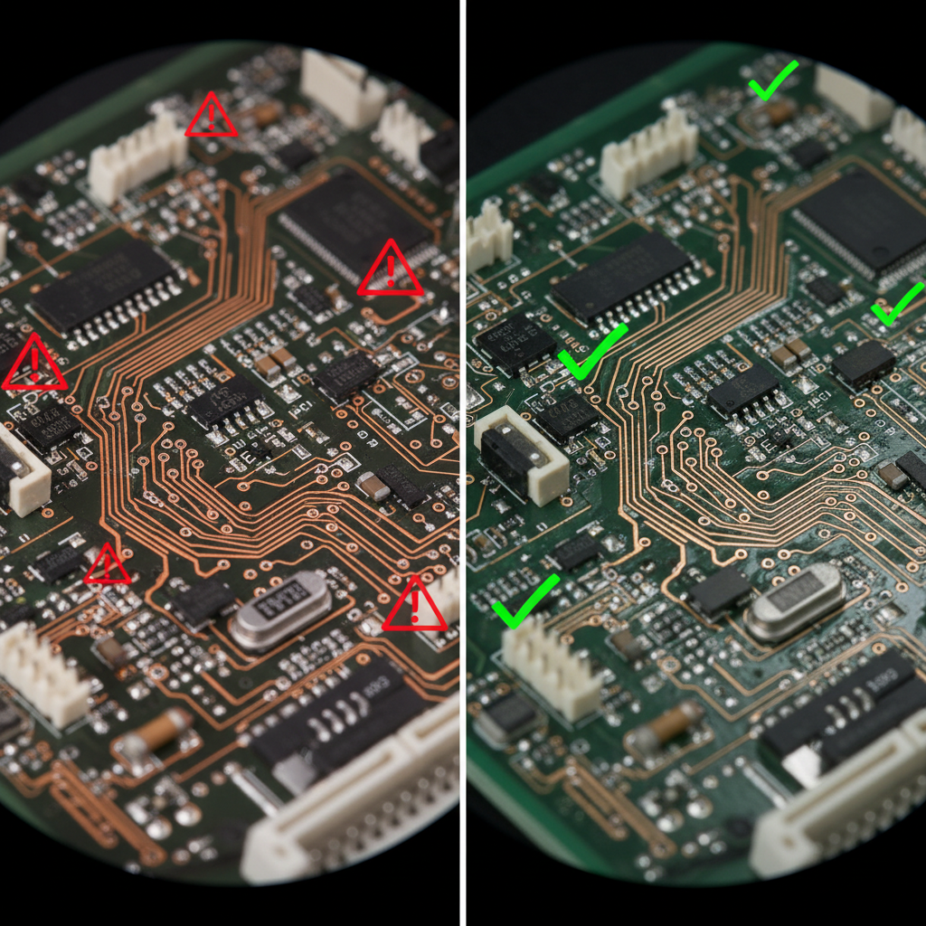
Design for Manufacturing (DFM) considerations ensure that the design can be reliably fabricated and assembled. This includes maintaining minimum trace widths and spacing that the manufacturer can consistently produce, placing components far enough from board edges to allow panelization, orienting components consistently to simplify automated assembly, and avoiding features that create manufacturing difficulties.
When an industrial controls manufacturer submitted designs with 0.075mm traces throughout the board, their PCB manufacturer flagged potential yield issues. While technically within capability, such fine traces increase fabrication costs and failure rates. The design service revised the layout, using 0.075mm traces only where necessary for routing density and wider traces elsewhere—a practical application of design-for-manufacturing principles that balance technical requirements with production realities. This simple change improved manufacturing yield by 15% without compromising functionality.
Essential Deliverables From Professional Design Services
Manufacturing-ready files encompass several document types, each serving specific purposes in the production process. Understanding these deliverables helps you evaluate whether a design service provides complete documentation.
Schematics document the electrical connections between components. Professional schematics use clear component designators, include design notes explaining critical decisions, and organize signals logically for easy review. These become the reference documentation for troubleshooting, repairs, and future design revisions.
Bills of Materials (BOMs) list every component on the board with manufacturer part numbers, quantities, and reference designators. Detailed BOMs include component descriptions, specifications, and approved alternates. This information enables accurate procurement and prevents assembly delays caused by ambiguous component specifications.
Layout files contain the complete physical design in formats like Altium, OrCAD, or KiCad native files. These allow future modifications without starting from scratch and provide the source data for generating manufacturing files.
Gerber files represent the industry-standard format for communicating PCB designs to manufacturers. Each Gerber file describes one layer of the board—top copper, bottom copper, soldermask, silkscreen, etc. Modern extended Gerber format (RS-274X) includes all necessary information in a single file per layer, making it the most reliable way to transfer designs between different CAD systems.
ODB++ format provides an alternative to Gerber files that includes additional manufacturing information in a single package. Some manufacturers prefer ODB++ because it includes layer relationships, component data, and design intent that separate Gerber files don’t convey.
Drill files specify hole locations, sizes, and types (plated or non-plated). These guide the drilling process that creates component holes and vias. Proper drill file generation includes appropriate tool sizes, hit optimization to minimize drilling time, and clear indication of which holes should be plated through.
Assembly drawings show component locations, orientations, and reference designators. These guide manual assembly and provide verification references for automated assembly. Professional assembly drawings include board outlines, critical dimensions, and notes about special handling requirements.
IPC-356 netlist files contain electrical connectivity information that enables automated electrical testing. These files allow manufacturers to verify that fabricated boards match the design intent before assembly.
Test point documents identify locations and signals for test access during production testing and troubleshooting. Well-placed test points simplify debugging and reduce manufacturing test time.
Manufacturing notes communicate special requirements like controlled impedance specifications, specific material requirements, special finishes, or tight tolerance callouts. Clear notes prevent misunderstandings that could compromise board performance.
When an aerospace contractor received their first prototype boards, they discovered the manufacturer had interpreted ambiguous drill specifications differently than intended. Several critical mounting holes were 0.5mm undersized, preventing mechanical assembly. The mistake cost two weeks while replacement boards were fabricated. Professional design services prevent such issues by providing comprehensive, unambiguous manufacturing documentation—the same attention to detail that drives success in PCB assembly partnerships.
Effective Collaboration With Your Design Service Provider
The relationship between your team and the PCB design service directly influences project success. Effective collaboration requires clear communication, well-defined processes, and mutual respect for each party’s expertise.
Start by providing comprehensive requirements documentation. Include electrical specifications, mechanical constraints, environmental conditions, certification requirements, and cost targets. The more information your design service has upfront, the fewer iterations you’ll need later. Don’t assume that “standard PCB” communicates enough—specify substrate materials, finish requirements, and any special considerations.
Establish regular communication channels and review milestones. Weekly design reviews keep projects on track and provide opportunities to catch issues early. During reviews, ask questions about design decisions you don’t understand. Professional designers welcome these discussions because they ensure everyone shares the same understanding of requirements and constraints.
Implement disciplined revision control from the beginning. Every design change should be documented with clear version numbers and change descriptions. This prevents confusion about which version represents the current design and provides an audit trail if questions arise during manufacturing or testing.
Schedule early Design for Manufacturing (DFM) reviews with your PCB manufacturer. Sending preliminary designs to your manufacturer before finalizing the layout allows them to identify potential fabrication issues while changes are still easy to implement. Manufacturers appreciate this proactive approach and can often suggest design modifications that improve yield or reduce cost without compromising performance.
A medical device company learned this lesson after their first production run had 30% yield due to soldermask registration issues with fine-pitch components. An early DFM review with their manufacturer would have identified the problem and allowed design modifications before production. After implementing early DFM reviews as standard practice, their first-pass yields improved to above 95%.
Consider partnering with manufacturers who offer integrated design support. Companies like Flex Plus provide both design consultation and manufacturing services, ensuring that designs are optimized for their specific fabrication processes. This integration eliminates the communication gaps that can occur when design and manufacturing are separate organizations.
Maintain open dialogue about cost and schedule tradeoffs. Professional design services understand that every project has budget and timeline constraints. Discussing these honestly allows designers to make appropriate compromises—perhaps using slightly wider trace spacing to improve yield, or selecting more readily available components to avoid lead time issues.
Document key decisions and requirements in writing. Email confirmations of verbal discussions prevent misunderstandings about what was agreed. This documentation becomes valuable if questions arise months later during production ramp-up.
Common Design Pitfalls That Sabotage Manufacturing
Even experienced engineers sometimes create designs that cause manufacturing headaches. Recognizing these common pitfalls helps you avoid them in your projects.
Insufficient design margins cause yield problems when manufacturing variations push parameters beyond limits. For example, designing trace widths at the absolute minimum capability leaves no margin for etch variation. If your manufacturer’s minimum trace width is 0.1mm, designing 0.15mm traces provides safety margin that improves consistency.
Poor component placement creates assembly difficulties, thermal issues, or mechanical problems. Components placed too close to board edges may be damaged during handling. Heat-generating components clustered together create hot spots. Connectors oriented inconsistently complicate cable routing. Professional designers consider the full lifecycle—fabrication, assembly, testing, installation, and maintenance—when placing components.
Inadequate via sizing and placement affects electrical performance and mechanical reliability. Vias that are too small may crack during thermal cycling, especially on flexible circuits. Insufficient via count for high-current paths causes voltage drops and heat buildup. Professional designs calculate required via sizes based on current requirements and include extra vias for reliability.
Missing or incorrect netlist management leads to connectivity errors that may not appear until electrical testing. When schematic changes aren’t properly synchronized with layout, the resulting design contains unintended connections or missing signals. Rigorous design rule checks and careful cross-verification between schematic and layout prevent these errors.
Ignoring flex circuit special requirements causes premature failures in flexible PCB applications. Flex circuits require special consideration for bend areas—no components or vias in dynamic flex regions, staggered trace layouts to distribute strain, and adequate copper thickness to handle repeated bending. Designers without flex PCB experience often create layouts that look fine but fail in actual use.
An automotive sensor manufacturer discovered this painfully when their flex cable assemblies began failing after 50,000 bend cycles, far short of the 1 million cycle requirement. Investigation revealed that the layout placed vias within the bend region and used parallel trace routing that concentrated stress. A professional flexible PCB design service redesigned the layout with staggered traces, moved vias outside the bend area, and selected appropriate copper weight. The revised design exceeded 2 million cycles without failures.
Inadequate ground plane design causes electromagnetic interference and signal integrity problems. Split ground planes, return current path discontinuities, and insufficient ground connections create both radiated emissions and susceptibility to interference. Professional designs include continuous ground planes, carefully manage plane splits near high-speed signals, and provide multiple ground connections for shields and connectors.
Overlooking manufacturing tolerances creates designs that work on paper but fail in production. Pad sizes that don’t account for registration tolerances lead to solder shorts. Tight-tolerance mechanical features may not align with actual manufacturing capabilities. Professional designers understand real-world manufacturing variations and design accordingly.
Choosing Your Design Partner for Manufacturing Success
The right PCB design service becomes a true engineering partner, not just a service provider. Look for organizations with deep manufacturing knowledge, not just design software proficiency. Ask about their experience with your specific application—medical devices, automotive electronics, industrial controls—because each domain has unique requirements and standards.
Evaluate their design processes and quality systems. ISO 9001 certification demonstrates commitment to documented processes and continuous improvement. For medical devices, ISO 13485 compliance is essential. Automotive applications require understanding of IATF 16949 standards. These certifications indicate that the design service understands the quality requirements your products must meet.
Consider the value of working with an integrated manufacturer-designer. When design and manufacturing exist under one roof, communication flows seamlessly, DFM reviews happen naturally, and your designs are automatically optimized for the specific fabrication processes that will produce them. This integration eliminates the translation errors and miscommunications that plague projects where design and manufacturing are separate organizations.
Flex Plus exemplifies this integrated approach, combining 20+ years of flexible PCB manufacturing expertise with comprehensive design support services. Their engineers understand not just how to draw traces, but how those traces perform through fabrication, assembly, and years of field use. This knowledge, backed by international certifications and proven across diverse applications from medical devices to electric vehicles, ensures that your designs are truly manufacturing-ready from the start.
The difference between adequate PCB designs and exceptional ones lies in understanding that design and manufacturing are inseparable. Your manufacturing-ready files don’t just describe what you want—they determine what you get. Investing in professional PCB design services, particularly from partners who control both design and fabrication, delivers the foundation for production success that no amount of downstream correction can match.