
The electronics industry stands at a pivotal moment. As devices shrink and functionality expands, engineers face an increasingly difficult challenge: how do you pack more capability into less space while maintaining reliability? The answer lies in ultra-thin flexible printed circuit boards—specifically, 25-micron flex circuits that are fundamentally changing what’s possible in wearables and medical implants.
These ultra-thin FPCBs represent more than incremental improvement. They’re enabling entirely new product categories. Smart patches that monitor vital signs continuously. Medical implants that conform perfectly to body contours. AR glasses light enough to wear all day. Each advancement depends on circuits thin enough to disappear yet robust enough to perform reliably for years.
At Flex Plus, we’ve spent over two decades perfecting ultra-thin FPCB manufacturing. Through this work, we’ve learned that achieving 25-micron thickness isn’t just about making things smaller—it’s about reimagining the entire manufacturing process, from material selection to final assembly. Let’s explore how these remarkable circuits work and what they make possible.
Materials and Stack-Up: The Foundation of Ultra-Thin Design
Creating a 25-micron flex circuit begins with material choices that would have seemed impossible a decade ago. The substrate forms the foundation, and polyimide remains the gold standard for ultra-thin applications. Unlike standard polyimide films at 50 or 75 microns, ultra-thin variants measure just 12.5 to 25 microns while maintaining the thermal stability and mechanical strength that make polyimide indispensable.
The copper foil presents an equally critical decision. Standard flex circuits typically use 18-micron (½ oz) copper, but ultra-thin designs often employ 9-micron or even 3-micron copper foils. This isn’t simply about reducing thickness—thinner copper creates challenges in current-carrying capacity and trace definition that demand careful engineering consideration.
Here’s where adhesiveless FCCL (Flexible Copper Clad Laminate) technology becomes transformative. Traditional flex circuits bond copper to polyimide using adhesive layers that add 15-25 microns of thickness. Adhesiveless construction eliminates this layer entirely, using direct metallization processes to bond copper atomically to the polyimide substrate. The result? Circuits that can achieve total thickness below 50 microns while offering superior flexibility and thermal performance.
A typical ultra-thin double-sided flex stack-up might comprise 12.5-micron polyimide, 9-micron copper on each side, and 15-micron coverlay—totaling just 45.5 microns before considering trace thickness. With gold plating for enhanced reliability, you can achieve finished assemblies under 50 microns that maintain excellent electrical performance.
Surface finish selection becomes especially important in ultra-thin designs. Electroless nickel immersion gold (ENIG) remains popular for its excellent solderability and shelf life, but the nickel layer’s stiffness can reduce flexibility in ultra-thin circuits. For maximum flexibility, immersion gold directly on copper or electroless palladium immersion gold (EPIG) offers alternatives. Each choice involves trade-offs between flexibility, solderability, cost, and long-term reliability.
Manufacturing Techniques: Precision at Micron Scale
Producing ultra-thin FPCBs demands manufacturing capabilities far beyond standard flex circuit fabrication. Photo-patterning forms the foundation—exposing photosensitive resist through precision masks, then etching unwanted copper. But at 25-micron total thickness, every process parameter becomes critical. Etch rates must be controlled within seconds. Resist adhesion must be perfect. Even temperature variations of a few degrees can affect dimensional accuracy.
Laser micro-machining adds another dimension of precision. Modern UV or CO2 lasers can cut features as small as 25 microns with minimal heat-affected zones. Recent advances in micron-scale electronics fabrication have enabled even finer precision for next-generation medical implants and wearable sensors. This capability proves essential for creating via holes in ultra-thin materials, where mechanical drilling would destroy the delicate substrate. Pulse lasers emit energy in short, high-intensity bursts, making them ideal for cutting extremely fine details without damaging surrounding material.
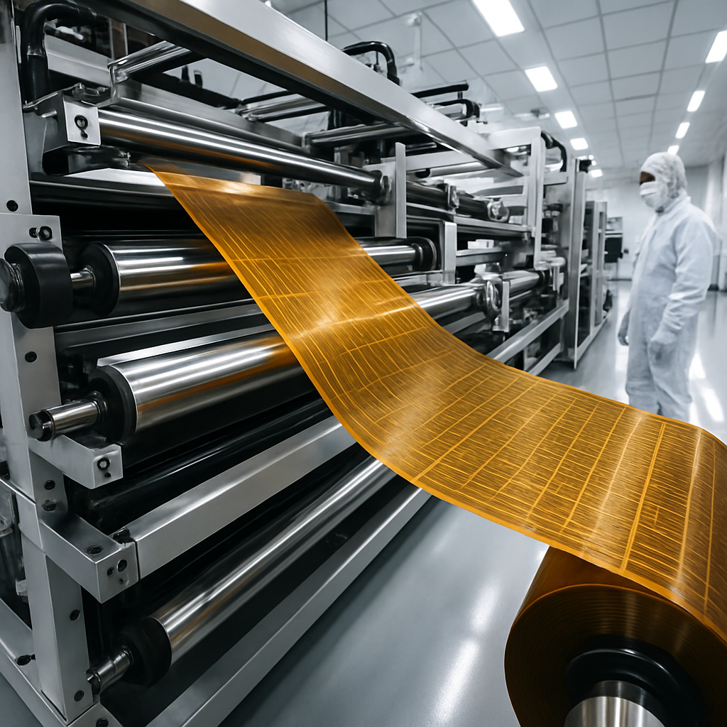
Roll-to-roll processing represents a breakthrough for high-volume ultra-thin FPCB production. Rather than processing individual panels, roll-to-roll systems handle continuous webs of material, enabling consistent quality across hundreds of meters. The entire web moves through sequential operations—lamination, exposure, etching, coating—with precise tension control maintaining dimensional stability throughout.
This continuous processing approach delivers multiple advantages for ultra-thin circuits. Material handling becomes gentler, reducing mechanical stress on delicate substrates. Process parameters remain more consistent across long production runs. Most importantly, roll-to-roll manufacturing enables cost-effective production of the long, narrow flex circuits increasingly common in wearables and medical devices.
At Flex Plus, our roll-to-roll capabilities extend to circuits up to four meters in length—critical for applications like medical monitoring systems where a single flex circuit must snake through an entire device assembly. This length capacity, combined with our ability to maintain line width/space down to 50 microns (2mil/2mil), enables designs previously considered impractical.
Design Rules and Electrical Considerations
Designing ultra-thin FPCBs requires rethinking conventional rigid PCB rules. Trace width and spacing constraints become more stringent as thickness decreases. While standard flex circuits might tolerate 100-micron (4mil) traces, ultra-thin designs with 9-micron copper often require minimum trace widths of 50-75 microns to maintain current capacity and manufacturing yield.
Current-carrying capacity decreases proportionally with copper thickness. A 9-micron copper trace carries roughly half the current of an 18-micron trace of the same width before reaching temperature limits. For power distribution in ultra-thin circuits, designers must either widen traces significantly or accept higher operating temperatures—both choices with system-level implications.
Impedance control presents unique challenges in ultra-thin stack-ups. The proximity of ground and signal layers, combined with thin dielectrics, creates high capacitance that lowers characteristic impedance. Achieving standard 50-ohm or 100-ohm differential impedance often requires wider traces than expected, consuming precious routing space. Careful simulation using accurate dielectric constants becomes essential—polyimide’s dielectric constant varies with thickness and adhesive presence.
Thermal management demands special attention in ultra-thin designs. The very thinness that enables device miniaturization also reduces thermal mass and heat spreading capability. Localized hot spots can develop quickly around high-power components or dense interconnects. For applications like wearables contacting skin, temperature rises must be carefully limited—often to just a few degrees above ambient.
Flex Plus has pioneered breakthrough solutions for thermal challenges in ultra-thin FPCBs through our proprietary flexible heat dissipation flow channels. By integrating thermal pathways directly into the flex circuit structure, we can reduce device operating temperatures significantly without adding bulk. This technology proves especially valuable in high-power LED applications and automotive electronics where thermal management determines device lifespan.
Mechanical Reliability: Designing for Durability
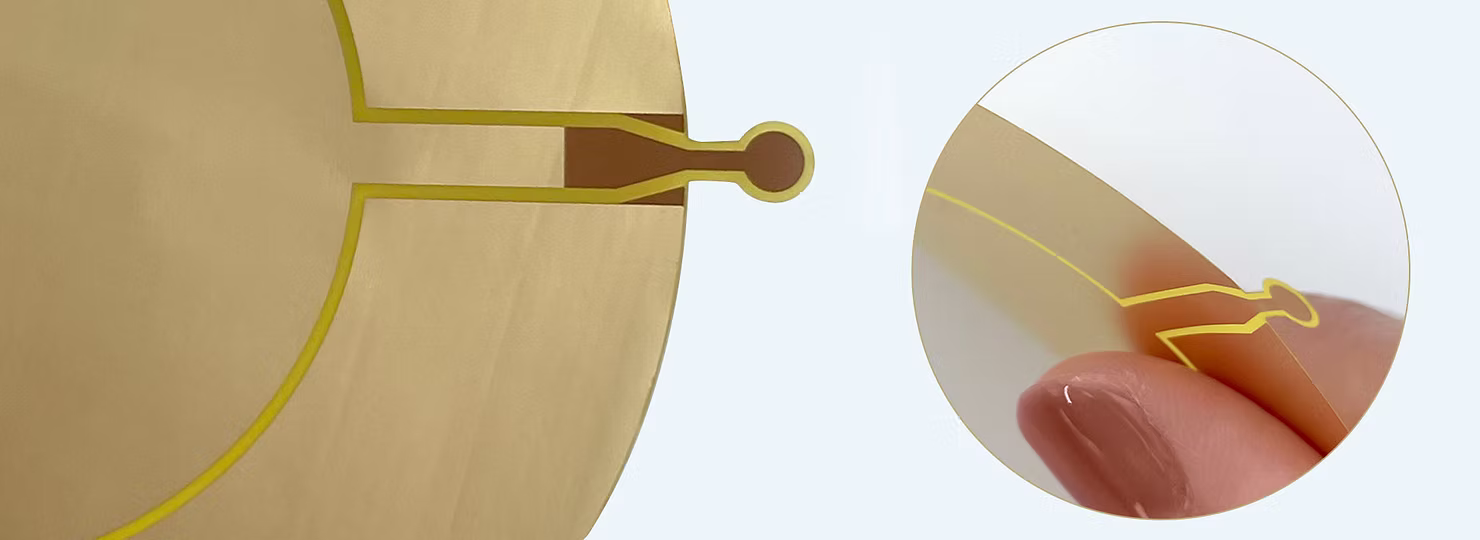
Ultra-thin flexibility creates both opportunities and challenges for mechanical reliability. On one hand, thinner circuits bend more easily with smaller bend radii—critical for wearables that must conform to body contours. A 25-micron circuit can achieve bend radii below 1mm, enabling integration into jewelry-sized devices or conforming to curved medical implant surfaces.
However, this extreme flexibility demands careful design to prevent mechanical failures. Bend lines—areas subjected to repeated flexing—require special attention. Traces crossing bend lines should run perpendicular to the bend axis when possible, minimizing the strain experienced during flexing. Understanding proper flexible circuit design guidelines prevents mechanical failures in high-flex applications. When parallel traces are unavoidable, staggering them across the bend zone distributes stress more evenly.
Material selection around bend areas matters enormously. Stiffer coverlay materials or surface finishes like ENIG can create stress concentration points that initiate cracks after thousands of flex cycles. For applications requiring millions of cycles—like smartwatch flex circuits—designers often specify softer coverlay materials or eliminate coverlay entirely in bend zones, leaving bare polyimide as the outer layer.
Strain relief becomes critical at transition points between flexible and rigid sections or where components mount. Stiffeners—rigid FR-4 or polyimide sections bonded to the flex—must extend far enough to prevent sharp bending at the transition. Teardrop pad geometries instead of abrupt angle corners reduce stress concentration at solder joints.
Dynamic bending applications—where the circuit flexes continuously during use rather than being bent once during assembly—present the most demanding reliability requirements. Wearable devices might experience 200,000 or more flex cycles during typical use. Medical implants must survive millions of cycles from body movement. Achieving this reliability demands not just proper design but also rigorous flex testing during development.
Assembly, Testing, and Yield Management
Handling ultra-thin flex circuits during assembly requires specialized techniques and equipment. These delicate circuits can tear, wrinkle, or deform with improper handling. Vacuum fixtures with gentle hold-down pressure prevent movement during component placement without damaging the substrate. Advanced SMT assembly techniques for FPCB ensure reliable component attachment on ultra-thin flexible substrates. Magnetic fixtures, a technology Flex Plus has pioneered, provide even pressure distribution across uneven surfaces—essential when assembling COB (Chip-on-Board) directly onto flex substrates.
SMT component placement on ultra-thin flex presents unique challenges. Standard vacuum nozzles can deform the flexible substrate during component placement, causing misalignment. Custom soft-touch tooling maintains position accuracy without damaging the circuit. Pick-and-place machines must compensate for minor substrate warping—inevitable with ultra-thin materials—through vision system feedback and real-time placement adjustment.
Reflow soldering requires careful thermal profiling. Ultra-thin circuits heat and cool more rapidly than rigid PCBs, creating narrower process windows. The substrate’s flexibility can cause components to shift during reflow if not properly fixtured. Vapor phase reflow offers advantages for ultra-thin assembly by providing more uniform heating and eliminating substrate warping from forced convection.
For applications requiring ultimate thinness and reliability, Flex Plus‘s COB capabilities prove invaluable. By bonding die directly to the flex substrate, we eliminate the thickness and rigidity of packaged components. Our industry-leading die bonding precision—with wafer offset angle tolerance within ±5°—ensures reliable interconnections even on curved or uneven flexible substrates. Encapsulation thickness tolerance of just ±25-50 microns maintains the ultra-thin profile critical for wearables and implants.
Testing ultra-thin FPCBs demands specialized approaches. Flying probe testers must use lighter touch pressure to avoid puncturing thin coverlay or deforming traces. In-circuit testing fixtures require careful design to make reliable contact without damaging delicate circuits. For high-volume production, bed-of-nails fixtures with spring-loaded probes provide the gentlest contact method, but custom fixture design becomes essential for each circuit design.
Yield management in ultra-thin FPCB production requires vigilant process control. Minor variations in etching time, exposure energy, or lamination pressure—negligible in standard flex manufacturing—can significantly impact yield with ultra-thin materials. Flex Plus‘s comprehensive DFMEA (Design for Manufacturing and Assembly) analysis identifies potential yield detractors before production begins, enabling design optimization that balances performance requirements with manufacturing reality.
Applications and Industry Impact
Ultra-thin FPCBs are enabling product categories that weren’t feasible with conventional electronics. In wearables, 25-micron circuits disappear beneath clothing or against skin, creating comfortable devices users actually wear consistently. Smart patches monitoring glucose levels or heart rhythms rely on ultra-thin flex circuits designed for wearable technology that move naturally with body motion, maintaining electrical contact without irritation even during exercise or sleep.
AR and VR devices represent another transformative application. Traditional displays require rigid PCB interconnects that add bulk and weight to head-mounted devices. Ultra-thin flex circuits—especially our transparent PCB technology with ≥90% optical clarity—enable displays and optics to be positioned closer to the eye while reducing device weight dramatically. For all-day AR glasses to succeed, every gram matters. Ultra-thin FPCBs contribute to weight reduction that makes comfortable, socially acceptable smart glasses possible.
Medical implants benefit profoundly from ultra-thin FPCB technology. Research on multifunctional bioelectronics demonstrates how flexible circuits enable both electrical communication and drug delivery in advanced medical devices. Cardiac monitoring devices, neural interfaces, and drug delivery systems all require electronics that can be implanted beneath skin or within body cavities with minimal tissue displacement. Twenty-five-micron flex circuits can be rolled into cylinder diameters under 3mm or conform perfectly to curved implant surfaces. Combined with our biomedical-compatible materials and ISO 13485 certification, these ultra-thin circuits enable medical devices that improve outcomes while minimizing patient discomfort.
The electric vehicle industry increasingly relies on ultra-thin flex circuits for battery management systems and sensor networks. Long-format circuits—up to four meters in Flex Plus‘s capabilities—can snake through vehicle assemblies while maintaining flexibility for assembly and service access. The space and weight savings prove especially valuable in EVs where every kilogram affects range and every cubic centimeter enables more battery capacity.
Challenges, Trade-offs, and Future Directions
Despite remarkable capabilities, ultra-thin FPCBs involve real trade-offs. Mechanical fragility remains the most obvious—these circuits can tear during handling or assembly if not properly supported. Designers must carefully consider how the circuit will be handled during production, where stiffeners are needed, and what bend radii will be experienced during use.
Manufacturing complexity translates to higher costs compared to standard flex circuits. Yield rates typically run lower for ultra-thin designs due to handling challenges and tighter process windows. For applications where 50-micron or 75-micron flex would suffice, the added cost of ultra-thin construction may not provide commensurate value. Smart design means using ultra-thin construction only where it’s truly necessary—perhaps in bend zones or under tight spatial constraints—while using more robust stack-ups elsewhere in the same circuit.
The future of ultra-thin FPCB technology points toward even thinner constructions and novel materials. Research into nanomaterials, including graphene-based flexible electronics and carbon nanotube interconnects, promises circuits potentially measured in single-digit microns. New substrate materials beyond polyimide—including ultra-thin liquid crystal polymer (LCP) films—offer improved high-frequency performance for 5G and beyond applications.
At Flex Plus, we’re continuously advancing ultra-thin FPCB capabilities through our commitment to innovation and engineering partnership. Our TPU (Thermoplastic Polyurethane) circuit technology represents one such breakthrough—combining medical-grade flexibility with ultra-thin construction for next-generation wearables and biomedical devices. As electronic devices continue their march toward miniaturization and body integration, ultra-thin FPCBs will enable possibilities we’re only beginning to imagine.
The electronics industry’s future is thin, flexible, and conformable. Whether it’s a medical implant monitoring heart function, AR glasses overlaying digital information on the physical world, or a smartwatch tracking your health 24/7, ultra-thin FPCBs form the invisible foundation enabling these technologies. For engineers and companies pushing the boundaries of what’s possible, partnering with a manufacturer offering proven ultra-thin FPCB expertise isn’t just an advantage—it’s essential to turning ambitious designs into reliable, manufacturable products.