
Every successful product begins with a conversation between design vision and manufacturing reality. For design engineers working on flexible PCB projects, this conversation starts long before the first prototype leaves the production floor. Understanding flexible PCB manufacturing solutions isn’t just about knowing technical specifications—it’s about preventing costly redesigns, ensuring reliability, and accelerating your product’s journey from concept to market.
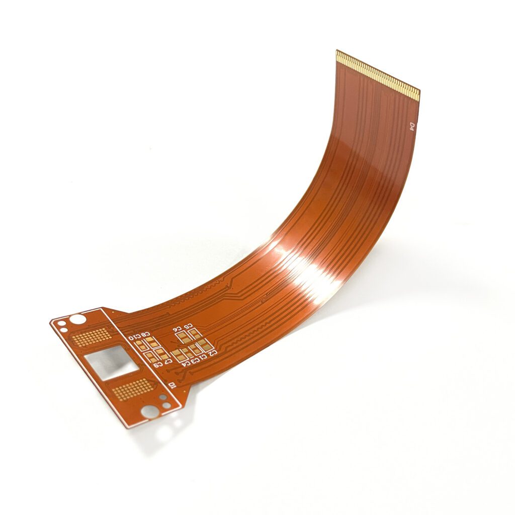
Flexible printed circuit boards (FPCs) and rigid-flex PCBs represent a fundamental shift from traditional rigid boards. These circuits can bend, fold, and twist while maintaining electrical integrity, making them essential for modern electronics where space is precious and reliability is non-negotiable. Whether you’re developing next-generation wearables, automotive sensors, or medical devices, the decisions you make during the design phase directly impact manufacturability, cost, and long-term product performance.
Understanding Materials and Stack-Ups: The Foundation of Reliable Flexible PCBs
Material selection forms the bedrock of any flexible PCB project. Unlike rigid boards where FR-4 dominates, flexible circuits require materials that can withstand repeated bending without fracturing or losing electrical performance. The most common substrate is polyimide (PI), a high-performance polymer that maintains flexibility across temperature extremes while offering excellent electrical insulation properties.
When selecting materials, you’re balancing several factors simultaneously. Polyimide substrates typically range from 12.5 to 75 microns in thickness, with thinner materials offering greater flexibility but requiring more careful handling during manufacturing. For applications demanding extreme miniaturization—think wearable medical sensors or smartphone displays—engineers increasingly specify ultra-thin constructions down to 25 microns with gold plating on double-sided designs.
Copper weight selection carries equal importance. Standard flexible circuits use 18-35 micron (½ to 1 oz) copper, but high-current applications may require up to 70 microns (2 oz). Here’s the trade-off: thicker copper improves current-carrying capacity but reduces flexibility and increases the minimum achievable trace width. A board designed with 70-micron copper won’t bend as easily as one with 18-micron copper, potentially creating stress points in dynamic applications.
Adhesive versus adhesiveless constructions represent another critical decision. Traditional flexible PCBs use acrylic adhesives to bond copper to the polyimide substrate, but these adhesives can degrade at high temperatures or in harsh chemical environments. Adhesiveless constructions, where copper is directly deposited onto the substrate, offer superior thermal performance and thinner profiles—ideal for automotive under-hood applications or high-reliability medical implants.
For rigid-flex designs, the stack-up becomes more complex. You’re essentially creating a hybrid structure where rigid sections provide mechanical support for connectors and components, while flexible sections enable three-dimensional routing and movement. A typical automotive sensor might use a 4-layer rigid-flex design: two rigid FR-4 sections connected by a 2-layer flexible polyimide section. The transition zones between rigid and flexible areas require careful engineering to prevent stress concentration and delamination.
The Manufacturing Journey: From Design Files to Finished Product
Understanding the manufacturing process helps you design circuits that are not just theoretically sound but practically producible. The journey begins when your Gerber files arrive at the manufacturing facility, but what happens next determines whether your design succeeds or requires expensive revisions.
Photolithography forms the core of flexible PCB manufacturing. The process starts with copper-clad polyimide laminate. A photosensitive film (photoresist) is applied to the copper surface, then exposed to UV light through a photomask containing your circuit pattern. The exposed areas either harden or become soluble depending on whether positive or negative resist is used. After development, the unwanted copper is etched away using chemical solutions, leaving your precisely defined circuit traces.
For double-sided flexible circuits, this process occurs on both sides with careful alignment between layers. Manufacturers use precision registration systems to ensure holes and traces on opposite sides align within tolerances as tight as ±0.05mm. When your design includes microvias or buried vias in multilayer constructions, laser drilling creates these tiny interconnections—some as small as 0.1mm in diameter.
The coverlay application follows, protecting exposed copper traces while leaving specific areas—such as contact pads—exposed. Engineers specify whether to use photoimageable coverlay for fine-feature designs or traditional film coverlays for cost-sensitive applications. Surface finishes like electroless nickel immersion gold (ENIG) or immersion silver then protect exposed pads from oxidation while ensuring reliable solderability.
Design-for-Manufacturability (DFM) best practices play a crucial role throughout this process. When your design violates manufacturing capabilities—perhaps specifying 0.03mm traces when the facility’s minimum is 0.05mm, or placing vias too close to bend areas—problems emerge. Leading manufacturers conduct comprehensive DFM reviews before production begins, identifying potential issues like insufficient spacing between traces, inadequate bend radius in flex areas, or pad geometries that may cause soldering problems during assembly.
A real-world example illustrates this principle: an engineer designing a flexible circuit for a medical wearable initially specified 0.04mm trace widths throughout the design to maximize routing density. During DFM review, the manufacturer identified that while achievable, this tight spacing would significantly reduce yield and increase cost. By slightly increasing trace widths to 0.06mm in non-critical areas, the design maintained functionality while improving manufacturability by approximately 40%, translating to lower unit costs and faster delivery.
Quality Assurance: Standards and Testing That Ensure Reliability
For design engineers, understanding quality standards isn’t academic—it directly impacts your product’s reliability and your company’s reputation. International standards provide the framework ensuring your flexible circuits perform consistently across production runs and meet industry-specific requirements.
IPC-6013 serves as the primary qualification and performance specification for flexible printed boards in North America. This standard defines three classes of products: Class 1 for general electronic products, Class 2 for dedicated service electronic products, and Class 3 for high-reliability electronic products where continued performance is critical. Medical devices and automotive applications typically require Class 3 compliance, meaning tighter tolerances, more rigorous testing, and comprehensive documentation.
For medical device manufacturers, ISO 13485 certification ensures the manufacturer maintains quality management systems specifically designed for medical devices. This becomes particularly important when designing implantable devices or diagnostic equipment where failures could endanger patient safety. Similarly, automotive engineers should verify their manufacturing partner holds IATF 16949 certification, demonstrating capability to meet the automotive industry’s stringent requirements for defect prevention and continuous improvement.
Testing protocols validate that your design performs as intended. Electrical testing verifies continuity and isolation using automated test equipment that checks every connection against your design files. For flexible circuits, dynamic flex testing becomes critical—samples undergo thousands or even millions of bend cycles to verify the circuit survives its intended application. A smartphone hinge circuit might require testing through 100,000 flex cycles, while a wearable medical sensor may need validation through 1 million cycles.
Thermal cycling tests subject assembled boards to extreme temperature variations, typically -40°C to +125°C, revealing potential failures from coefficient of thermal expansion mismatches between materials. Microsectioning analysis examines cross-sections of the board under high magnification, verifying copper thickness, plating quality in vias, and proper lamination between layers.
For engineers, specifying the appropriate testing level balances reliability requirements against cost and schedule. A consumer electronics product with a 2-year expected lifespan requires less rigorous testing than an automotive sensor that must function flawlessly for 15 years in harsh conditions. Working with manufacturers who understand these trade-offs and can recommend appropriate testing protocols prevents both over-engineering and under-testing.
Innovation in Flexible PCB Technology: HDI and Beyond
The flexible PCB industry continues advancing rapidly, driven by demands for smaller, lighter, and more capable electronic devices. High-Density Interconnect (HDI) technology represents one of the most significant developments, enabling unprecedented miniaturization while increasing functionality.
HDI flexible circuits use microvias—laser-drilled holes typically 0.1 to 0.15mm in diameter—instead of traditional mechanical vias. These tiny interconnections allow significantly tighter trace routing and enable stacked via structures where multiple layers connect through a small footprint. For smartphone manufacturers, HDI technology enables routing between increasingly dense component packages while maintaining signal integrity at high frequencies.
The practical impact is substantial. A traditional flexible circuit for a smartphone camera module might use 0.1mm traces with 0.1mm spacing, limiting routing density. An HDI equivalent could achieve 0.05mm traces with 0.05mm spacing, effectively doubling the routing capacity in the same area. This capability becomes critical as smartphones pack more sensors, cameras, and antennas into shrinking device volumes.
Transparent PCB technology opens entirely new application possibilities. With transparency exceeding 90%, these specialized circuits enable integration into AR/VR displays, heads-up displays for automotive applications, and next-generation wearables where the circuit itself becomes part of the visual experience. Engineers working on augmented reality glasses, for instance, can now design flexible circuits that mount directly onto optical components without obstructing the user’s view.
Thermal management innovations address one of flexible circuits’ persistent challenges: heat dissipation. Traditional flexible circuits struggle with thermal management because the thin polyimide substrates offer limited heat spreading. New solutions incorporate embedded thermal pathways or specialized materials with enhanced thermal conductivity, enabling flexible circuits in high-power LED applications or automotive power electronics where managing heat determines reliability.
One breakthrough gaining traction involves flexible circuits on thermoplastic polyurethane (TPU) substrates. These medical-grade materials combine the flexibility of traditional polyimide with enhanced biocompatibility and a softer feel—ideal for wearable health monitors or smart clothing applications. TPU circuits can be made as thin as 0.15mm while supporting circuit layers with 18-70 micron copper, maintaining electrical performance while achieving the comfort levels consumers demand from wearables.
Evaluating Manufacturing Partners: A Practical Checklist
Selecting the right manufacturing partner might be the most consequential decision you make for your flexible PCB project. The differences between manufacturers go far beyond price—they fundamentally impact your product’s success and your engineering team’s efficiency.
Start by verifying direct manufacturing capabilities versus broker relationships. Some companies position themselves as flexible PCB suppliers but actually broker work to various factories, introducing communication delays, quality inconsistencies, and longer lead times. Direct manufacturers with end-to-end control over production enable you to communicate directly with production engineers, see real-time process updates, and receive faster responses when issues arise.
Engineering support separates adequate manufacturers from exceptional partners. Look for teams offering comprehensive Design-for-Manufacturability reviews before production begins. The best manufacturers analyze your design files, identify potential manufacturing challenges, and recommend specific improvements—not just generic suggestions but detailed feedback like “moving this via 0.2mm from the bend area will improve reliability by 60%.” This proactive approach prevents expensive redesigns and accelerates your path to production.
Certification portfolio reveals a manufacturer’s commitment to quality and their capability to serve specific industries. For medical device projects, verify ISO 13485 certification and ask about their experience with FDA-regulated products. Automotive applications demand IATF 16949 certification, while ISO 14001 demonstrates environmental management commitment—increasingly important for companies with sustainability requirements.
Technical capabilities should align with your product requirements, both current and future. If your roadmap includes HDI designs, verify the manufacturer can achieve 0.05mm traces and 0.1mm microvias. For products requiring long flexible circuits—perhaps LED lighting systems or industrial sensors—confirm they can handle lengths up to 3-4 meters if needed. Don’t just match current specifications; consider whether they can support your next-generation products without forcing a manufacturer change later.
Assembly services streamline your supply chain and reduce risk. Manufacturers offering complete Flex PCBA (printed circuit board assembly) services handle component procurement, surface mount technology (SMT) placement, and final testing—eliminating the need to coordinate between a board fabricator and a separate assembly house. This integration typically reduces lead times by 30-40% while ensuring optimal compatibility between board design and assembly processes.
Lead time flexibility matters when managing product launches. Standard production runs might allow 1-week turnaround, but what happens when you need emergency prototypes for a critical design review? Manufacturers offering 3-day emergency service give you the agility to respond quickly when schedules compress or design iterations require rapid turnaround.
The Value of End-to-End Solutions: Integration That Accelerates Success
The most successful flexible PCB projects share a common characteristic: integrated partnerships between design engineers and manufacturing teams from concept through mass production. This end-to-end approach transforms manufacturing from a transactional relationship into a strategic collaboration that reduces risk, optimizes costs, and accelerates time-to-market.
Consider the alternative scenario many engineers face: designing circuits in isolation, sending files to a manufacturer for quotes, discovering design changes are needed, iterating through multiple revision cycles, then starting over with assembly quotes and coordination. Each handoff introduces delays and potential for miscommunication. When design, fabrication, and assembly live under one roof with coordinated processes, these friction points disappear.
Integrated solutions enable concurrent engineering where manufacturing feedback informs design decisions in real-time. Instead of completing your entire design before receiving DFM feedback, you work collaboratively with manufacturing engineers throughout the development process. This approach catches issues earlier when changes cost less and hurt schedules less. A via placement problem discovered during design review takes minutes to fix; the same issue discovered during prototype fabrication costs days or weeks.
Cost optimization improves through integrated understanding of how design choices impact manufacturing economics. An experienced manufacturing partner can explain that slightly increasing your minimum trace width from 0.05mm to 0.06mm might reduce your unit cost by 15% while maintaining full functionality. Or that consolidating from a 6-layer to a 4-layer design through thoughtful re-routing could cut material costs by 30%. These insights come from manufacturers who understand both design requirements and production realities.
Quality improves when the same team responsible for fabrication handles assembly. Board-level design decisions impact assembly success—pad sizes affect soldering reliability, component placement near flex areas influences mechanical stress, and surface finish selection determines assembly yield. When fabrication and assembly teams collaborate from the start, they optimize the entire product holistically rather than treating board and assembly as separate problems.
For companies scaling from prototypes to volume production, end-to-end partners provide continuity that prevents the common pitfall of “prototype-to-production redesign.” Designs optimized for low-volume prototype processes often don’t translate efficiently to high-volume manufacturing. Partners with capability across this entire spectrum design with volume production in mind from the beginning, ensuring your prototype is truly representative of production units rather than requiring substantial redesign for manufacturability.
The philosophy of integrated excellence recognizes that flexible PCB manufacturing isn’t just about producing boards to specification—it’s about enabling your innovation through technical expertise, comprehensive support, and manufacturing processes that align with your business goals. Twenty years of specialized experience, international certifications including ISO 9001, ISO 13485, and IATF 16949, and end-to-end capabilities from raw materials to final assembly create the foundation for this partnership approach.
As you prepare your next flexible PCB project for production, remember that the decisions you make before manufacturing begins—material selection, manufacturing partner evaluation, design optimization—determine whether your product succeeds quickly and cost-effectively or struggles through expensive iterations. By understanding manufacturing realities and partnering with the right team, you transform potential obstacles into competitive advantages, bringing your innovative designs to life with confidence.