
The modern world demands more from less. As technology advances, devices become smaller, more powerful, and increasingly sophisticated. This paradox—achieving greater functionality within tighter spaces—has driven one of the most transformative innovations in electronics: folding electronics design. This revolutionary approach is reshaping industries from medical devices to electric vehicles, from wearable technology to aerospace applications.
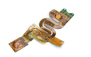
Folding electronics design represents a fundamental shift in how we conceptualize circuit boards. Unlike traditional rigid printed circuit boards that maintain fixed shapes, foldable circuit boards are engineered to bend, flex, and fold without compromising their electronic pathways. This capability isn’t merely a convenience—it’s becoming essential as manufacturers across industries seek solutions that fit into increasingly compact and irregular spaces.
The demand for folding electronics has exploded in recent years. Smartphones that fold in half, medical implants that conform to body contours, and automotive displays that wrap around dashboards all rely on this technology. According to industry projections, the flexible PCB market continues its rapid expansion, driven by applications in electric vehicles, wearable devices, and next-generation consumer electronics. These aren’t niche products anymore—they’re mainstream solutions addressing real-world constraints.
Consider the electric vehicle industry, where every millimeter of space matters. Head-up displays, side camera modules, and sensor arrays must fit within aerodynamic designs while maintaining reliability under constant vibration and temperature fluctuations. Traditional rigid boards simply cannot accommodate these requirements. Folding electronics provide the answer, enabling three-dimensional circuit routing that maximizes functionality while minimizing footprint.
The Foundation: Circuit Architecture and Flexible PCBs
At the heart of folding electronics lies a sophisticated marriage of circuit architecture and material science. Flexible printed circuit boards, commonly known as flex PCBs, form the backbone of this technology. Unlike their rigid counterparts constructed from fiberglass-reinforced epoxy, flex PCBs utilize specialized materials that maintain electrical integrity while bending, twisting, and folding.
The most common substrate material is polyimide, a remarkable polymer that combines exceptional flexibility with outstanding thermal stability. Polyimide can withstand temperatures exceeding 200°C while maintaining its flexibility across a wide temperature range. This makes it ideal for applications from medical devices that undergo sterilization to automotive electronics exposed to engine compartment heat.
On this flexible substrate, copper traces and pads are precisely etched using advanced manufacturing processes. The challenge isn’t simply creating conductive pathways—it’s ensuring these pathways survive thousands or even millions of bending cycles without failure. For double-sided flex PCBs with high circuit density, engineers must carefully consider how mechanical stresses during bending impact circuit traces between flex layers. The copper thickness, trace width, and routing patterns all influence the board’s flexibility and reliability.
Modern flex PCBs can achieve remarkable precision. Leading manufacturers now produce circuits with line widths and spacing as fine as 2/2 mils (approximately 50 micrometers), enabling high-density designs previously impossible with flexible substrates. This precision allows complex electronic functions to be packed into incredibly small form factors.
The architecture of flexible circuits extends beyond simple single-layer designs. Multi-layer flex PCBs stack multiple flexible circuits with insulating layers between them, creating sophisticated three-dimensional circuit routing. Some applications require rigid-flex PCBs—hybrid structures combining rigid sections for component mounting with flexible sections for bending and folding. These rigid-flex boards eliminate connectors between separate PCBs, reducing weight, improving reliability, and enabling more compact overall designs.
For applications involving repeated folding or dynamic flexing—such as foldable smartphones or wearable health monitors—the circuit architecture must account for mechanical fatigue. Engineers design trace patterns that distribute stress evenly, avoiding sharp corners or narrow necks where cracks might initiate. The goal is creating circuits that maintain electrical performance through tens of thousands of folding cycles.
The manufacturing precision required for these circuits is extraordinary. Advanced fabrication facilities control every parameter from copper plating thickness to coverlay adhesion strength. Quality control includes electrical testing, automated optical inspection, and often destructive testing of sample boards to verify bend reliability.
Designing the Foldable Future: From Concept to Prototype
Creating effective folding electronics requires a methodical design process that balances electrical performance, mechanical reliability, and manufacturing feasibility. This journey begins long before any physical prototype exists—it starts with three-dimensional modeling.
3D modeling software allows engineers to visualize how circuits will behave when folded into their final configurations. This virtual prototyping reveals potential problems early. Will components collide when the board folds? Do trace patterns create stress concentrations? Is there sufficient bend radius to prevent copper fracture? Answering these questions digitally saves considerable time and expense compared to discovering issues in physical prototypes.
Material selection happens concurrently with circuit design. While polyimide remains the dominant substrate material for its excellent flexibility and temperature resistance, specific applications may require alternatives. Medical devices might need biocompatible materials that won’t trigger immune responses. Wearable devices could benefit from stretchable substrates like thermoplastic polyurethane (TPU), which can accommodate not just bending but actual stretching—a capability useful in smart clothing and health monitoring patches.
The copper foil thickness significantly impacts both flexibility and performance. Thinner copper (18-35 micrometers) provides greater flexibility but limits current-carrying capacity. Thicker copper (70 micrometers or more) handles higher currents but reduces flexibility. Engineers must optimize this trade-off based on the application’s electrical requirements and expected mechanical stress.
Design for Manufacturing (DFM) analysis plays a critical role in successful folding electronics. This process reviews the circuit design against manufacturing capabilities and limitations, identifying potential problems before production begins. DFM analysis might reveal that trace spacing is too aggressive for reliable etching, that via placement could cause delamination during flexing, or that component placement interferes with fold lines.
Once the design passes DFM review, prototype development begins. Initial prototypes allow engineers to validate their assumptions about mechanical behavior and electrical performance. These early samples undergo rigorous testing—electrical continuity checks, impedance measurements, thermal cycling, and most importantly, dynamic bending tests.
Dynamic bending tests simulate real-world usage by repeatedly folding the circuit through its expected range of motion. Test equipment can cycle prototypes through thousands of folds while monitoring electrical parameters in real-time. Any degradation in performance indicates potential reliability issues requiring design modifications.
Iterative refinement follows initial testing. Perhaps the bend radius needs adjustment. Maybe trace routing requires modification to reduce stress concentration. The component layout might need rethinking to better accommodate the folded configuration. Each iteration brings the design closer to optimal performance and manufacturability.
User interaction considerations also influence the design process, particularly for consumer products. How will people actually fold the device? What tactile feedback should the mechanism provide? Does the folded state feel secure or fragile? These human factors affect not just the circuit design but also protective coverlay materials and overall construction.
Real-World Applications: From Origami Inspiration to Practical Innovation
The theoretical elegance of folding electronics becomes truly impressive when examining real-world applications. Across diverse industries, engineers are leveraging flexible and foldable circuit designs to solve problems previously considered insurmountable.
Researchers have developed origami-based electronic systems that take inspiration from the ancient Japanese art of paper folding. These origami electronic membranes can change shapes, provide multi-modal sensing, and switch functions through mechanical reconfiguration. One fascinating approach involves kiri-origami structures—combining cutting (kiri) with folding (origami)—which enable mounting rigid surface-mount devices on fundamentally flexible substrates. By strategically cutting patterns into flexible circuits, engineers create structures that stretch and fold while accommodating traditional electronic components.
This hybrid kiri-origami approach represents a paradigm shift. Previously, designers faced a stark choice: use flexible circuits with limited component options or use rigid boards with mounting restrictions. The kiri-origami technique allows large-area electronic devices to incorporate conventional components while maintaining flexibility. When stretched, the cut patterns open like a lattice, distributing strain across the structure rather than concentrating it in the copper traces.
The medical device industry has embraced folding electronics enthusiastically. Implantable sensors now conform to curved body surfaces, monitoring vital signs with minimal patient discomfort. One particularly innovative application involves flexible circuits with integrated microfluidic channels for drug delivery systems that can be folded into compact shapes for insertion, then expand to their functional configuration inside the body. Surgical tools incorporate flexible circuits that navigate through small incisions, enabling minimally invasive procedures. One particularly innovative application involves flexible circuits with integrated microfluidic channels for drug delivery systems that can be folded into compact shapes for insertion, then expand to their functional configuration inside the body.
Electric vehicles showcase folding electronics in demanding automotive environments. Modern EVs feature flexible circuits in battery management systems that conform to curved battery packs, in heads-up displays that follow windshield contours, and in door panels where circuits fold around hinges and structures. These applications must withstand extreme temperature swings, constant vibration, and years of reliable operation—requirements that push folding electronics technology to its limits.
The telecommunications industry has found folding electronics indispensable for 5G infrastructure. Optical transceiver modules use flexible circuits to route high-speed signals through compact spaces while managing thermal challenges. The flexibility allows optimal heat dissipation pathways that would be impossible with rigid boards.
Consumer electronics represent perhaps the most visible application of folding technology. Foldable smartphones have transitioned from concept to reality, featuring displays and circuits that fold thousands of times throughout the device’s lifetime. These products demonstrate the maturity of folding electronics technology—they’re not laboratory curiosities but consumer products sold globally and used daily.
Wearable technology pushes the boundaries further. Smart watches, fitness trackers, and even smart clothing incorporate flexible circuits that move naturally with the human body. Some advanced wearables use stretchable circuits based on TPU substrates, accommodating not just bending but actual elongation as muscles flex and joints bend. These devices collect health data, monitor environmental conditions, and provide real-time feedback—all while remaining comfortable and unobtrusive.
The aerospace sector applies folding electronics in satellite deployable structures, where circuits must survive launch stresses then unfold in space. These applications demand ultra-reliable designs that function in vacuum conditions with extreme temperature cycling. Similar technology appears in drone systems and emerging electric vertical takeoff and landing (eVTOL) aircraft, where weight savings and space efficiency directly impact flight performance.
Enabling Tomorrow’s Innovations: The Philosophy of Flexible Excellence
The revolution in folding electronics design doesn’t happen in isolation. It requires manufacturers who combine technical expertise with unwavering commitment to quality and innovation. This is where companies like Flex Plus (Xiamen) Co., Ltd play a crucial enabling role.
Since 2004, Flex Plus has specialized in advanced flexible and rigid-flex PCB solutions, developing deep expertise across diverse applications. Their approach exemplifies what’s necessary to support the folding electronics revolution: certified manufacturing excellence, genuine innovation capability, and complete manufacturing control.
Certification matters immensely in flexible electronics. Applications in medical devices require ISO 13485 compliance, ensuring biocompatible materials and processes meet stringent healthcare standards. Automotive electronics demand IATF 16949 certification, guaranteeing the quality systems necessary for components that must function reliably in safety-critical applications. These aren’t merely bureaucratic requirements—they represent systematic approaches to quality that ensure folding electronics perform as designed throughout their operational lives.
Innovation extends beyond simply manufacturing what others design. True innovation means developing breakthrough capabilities that enable entirely new applications. Consider flexible substrate Chip-on-Board (COB) technology, where ultra-thin chips mount directly onto flexible circuits. This integration achieves unprecedented compactness—total thickness can be reduced to mere hundreds of micrometers while maintaining full functionality. Such integration makes possible medical implants that were previously too bulky, consumer electronics with novel form factors, and industrial sensors that fit into spaces conventional packaging cannot reach.
The precision required for advanced COB on flexible substrates is remarkable. Die bonding tolerances must be controlled within ±5 degrees of rotation and positioning accuracy measured in micrometers. Encapsulation thickness uniformity reaches ±5 micrometers for dam structures and ±25-50 micrometers for overall packaging. This precision isn’t achievable without sophisticated equipment and, more importantly, deep process expertise developed over thousands of production cycles.
Complete manufacturing control distinguishes genuine manufacturers from brokers or trading companies. When a single facility handles everything from raw material processing through final testing, quality control becomes truly comprehensive. Problems get identified and resolved quickly rather than lost in communication between disparate suppliers. Engineering feedback loops tighten, accelerating the iterative refinement process essential for optimizing folding electronics designs.
Manufacturing capability must scale from prototyping through mass production. A design that works perfectly in small quantities might fail when scaled to thousands or millions of units. Manufacturers supporting the folding electronics revolution need facilities capable of rapid prototyping—delivering initial samples within days—while also handling high-volume production with consistent quality. This flexibility allows customers to move seamlessly from concept validation through product launch without changing suppliers.
The philosophy underlying successful flexible electronics manufacturing emphasizes partnership rather than transaction. Engineers at flexible circuit manufacturers become extensions of their customers’ design teams, providing technical guidance on material selection, offering DFM feedback to improve manufacturability, and suggesting design optimizations based on production experience. This collaborative approach reduces development risk and accelerates time-to-market.
Environmental responsibility also matters increasingly. ISO 14001 certification demonstrates commitment to minimizing environmental impact through systematic management of manufacturing processes. As folding electronics enable more sustainable product designs—lighter vehicles, more efficient electronics, less material waste—the manufacturers producing these circuits should themselves operate sustainably.
Looking forward, the folding electronics revolution continues accelerating. New materials promise even greater flexibility and reliability. Manufacturing processes advance toward finer features and higher precision. Applications expand into areas barely imagined a decade ago—from flexible displays that roll up like paper to bio-integrated electronics that interface directly with neural tissue.
These advances require manufacturers who don’t simply react to customer specifications but actively push technological boundaries. Innovation in materials, processes, and integration techniques enables designers to imagine and create products that weren’t previously possible. This virtuous cycle—where manufacturing capability enables design innovation which drives demand for advanced manufacturing—propels the entire industry forward.
The compact deployment enabled by folding electronics design represents more than clever engineering—it’s fundamentally changing what’s possible in electronic product design. As devices become smaller, lighter, and more capable, the flexible circuits that enable this transformation become increasingly critical. Success in this space requires not just following standards but setting them, not just meeting specifications but exceeding them, and not just manufacturing products but enabling innovation.
This is the philosophy that drives leaders in flexible PCB manufacturing: viewing each project as an opportunity to advance the state of the art, each customer relationship as a partnership in innovation, and each challenge as a chance to develop capabilities that will benefit the entire industry. As folding electronics continue revolutionizing space-constrained innovation across industries from medical devices to electric vehicles, from consumer electronics to aerospace, the manufacturers who enable this revolution through certified excellence, genuine innovation, and unwavering quality commitment will shape the technology landscape for decades to come.