
In today’s fast-paced electronics industry, the difference between a breakthrough product and a market failure often comes down to one critical decision: choosing the right manufacturing partner for your custom flexible PCB. Whether you’re developing the next generation of electric vehicles, life-saving medical devices, or cutting-edge aerospace technology, your PCB manufacturing partner isn’t just a supplier—they’re a cornerstone of your innovation strategy.
Consider this: a leading EV manufacturer recently launched a revolutionary head-up display system that required flexible circuits capable of withstanding extreme temperature fluctuations while maintaining perfect signal integrity. Their initial prototype partner couldn’t deliver the precision needed, resulting in six months of delays and nearly $2 million in additional development costs. When they switched to a certified flexible PCB specialist with proven automotive expertise, they brought their product to market in just four months.
This story isn’t unique. Across industries—from medical device companies developing biocompatible implants to telecommunications firms pushing the boundaries of 5G infrastructure—the manufacturing partner you choose directly impacts your product’s success, your time to market, and ultimately, your competitive advantage.
Understanding Custom Flexible PCBs: The Foundation of Modern Electronics
Custom flexible PCBs represent a revolutionary approach to circuit board design that has fundamentally changed how we think about electronic devices. Unlike traditional rigid boards made from FR-4 materials, flexible PCBs are composed of copper-clad polyimide films that can bend, twist, and fold without compromising electrical performance or mechanical integrity.
The magic of flexible PCBs lies in their unique construction. These circuits typically feature ultra-thin copper layers—ranging from 18 to 70 micrometers—laminated onto flexible polyimide substrates. This combination creates a circuit board that weighs up to 70% less than rigid alternatives while maintaining excellent electrical properties and thermal stability across a wide temperature range, from -200°C to +400°C.
What makes custom flexible PCBs particularly valuable is their adaptability. In a smartphone, for example, a flexible circuit connects the display to the main logic board while folding into a tight Z-shape that fits within millimeters of space. In an electric vehicle, these circuits snake through door panels and dashboards, connecting sensors, cameras, and control systems without the bulky connectors and rigid boards that once dominated automotive electronics.
The lightweight nature of flexible PCBs isn’t just about saving space—it’s about enabling entirely new product categories. Consider wearable medical devices that monitor patients’ vital signs 24/7. These devices require circuits that move with the body, withstand repeated flexing, and remain comfortable against skin for extended periods. Traditional rigid PCBs simply cannot meet these requirements, but custom flexible circuits make these innovations possible.
The Manufacturing Process: Where Expertise Makes All the Difference
The journey from design concept to finished flexible PCB is far more complex than many engineers realize, and this is where your manufacturing partner’s expertise becomes invaluable. The process begins with material selection—a critical decision that impacts everything from flexibility and durability to electrical performance and cost.
Polyimide remains the substrate of choice for most high-performance applications due to its exceptional thermal stability and mechanical properties. However, selecting the right polyimide grade, copper foil type, and adhesive system requires deep knowledge of how these materials behave under different conditions. A medical device requiring biocompatibility needs different material specifications than a telecommunications component operating in harsh outdoor environments.
The fabrication process itself demands precision at every step. After cutting the copper-clad laminate to size, manufacturers apply photoresist, expose circuit patterns using advanced imaging techniques, and etch away unwanted copper. For single-layer boards, this might seem straightforward, but multilayer flexible PCBs—which can stack up to eight layers in advanced applications—require laser-aligned via drilling with tolerances measured in micrometers.
Consider the challenge of creating a double-sided flexible PCB with line widths and spacing of just 2 mils (approximately 50 micrometers). At this scale, even minor variations in etching chemistry, exposure time, or temperature can result in open circuits or shorts. Advanced manufacturers invest in controlled environments with temperature regulation within ±2°C and humidity control to ensure consistent results.
The coverlay application and final profiling stages present their own challenges. Laser cutting technology has revolutionized flex PCB profiling, enabling complex shapes and tight tolerances that mechanical cutting cannot achieve. But laser parameters must be precisely tuned to avoid damaging the polyimide substrate or creating rough edges that could affect assembly.
Quality control throughout this process separates excellent manufacturers from mediocre ones. Leading facilities employ automated optical inspection (AOI) systems that scan every board at multiple stages, catching defects invisible to the human eye. Electrical testing verifies that every trace conducts properly and that insulation between layers meets IPC testing standards. Without rigorous quality control, even the best design can fail in production.
Applications Driving Innovation: From Space to Your Wrist
The versatility of custom flexible PCBs has opened doors across industries that were once limited by rigid board constraints. In the rapidly growing electric vehicle sector, flexible circuits have become indispensable. Modern EVs incorporate dozens of camera systems—from side mirrors and parking sensors to advanced LiDAR units—each requiring flexible interconnects that withstand vibration, temperature extremes, and constant flexing as doors open and mirrors adjust.
One particularly innovative application involves using ultra-thin flexible PCBs in vehicle wing mirror cameras. These circuits must fit within the streamlined housing while maintaining perfect signal integrity for high-resolution video feeds. They endure temperature swings from -40°C on winter mornings to over 80°C in summer sun, all while flexing thousands of times as mirrors fold. Only certified automotive-grade flexible PCBs can meet these demanding requirements.
The medical device industry represents another frontier where flexible PCB innovation saves lives. Biocompatible flexible circuits enable implantable devices like cardiac monitors and neural stimulators that must function flawlessly inside the human body for years. These applications demand ISO 13485 certification and materials proven safe for long-term contact with tissue. A manufacturing partner without specific medical device expertise simply cannot provide the documentation, traceability, and validation protocols required for regulatory approval.
In the emerging field of low-altitude airspace technology—including drones, electric vertical takeoff and landing (eVTOL) vehicles, and air taxis—flexible PCBs enable the lightweight, high-reliability systems essential for flight safety. A commercial drone delivery system might incorporate flexible circuits in its gimbal-mounted camera, landing sensors, and communication modules. Each circuit must be extremely lightweight to maximize payload capacity while meeting aerospace-grade reliability standards.
The beauty tech industry showcases how flexible PCBs enable entirely new product categories. Smart skincare devices that combine LED therapy, microcurrent stimulation, and temperature control require flexible circuits that conform to facial contours while delivering precise electrical signals. These applications demand ultra-thin designs—sometimes as thin as 25 micrometers with gold plating—that traditional manufacturing approaches cannot achieve.
Wearable technology and augmented reality devices push miniaturization even further. Smart helmets for F1 racing integrate heads-up displays, biometric sensors, and communication systems within the tight confines of a helmet shell. AI-powered glasses pack computing power, cameras, and displays into frames barely thicker than traditional eyewear. These applications require not just flexible PCBs, but rigid-flex designs that combine the structural stability of rigid boards with the space-saving flexibility of flex circuits.
The telecommunications industry continues evolving with 5G infrastructure demanding ever-smaller, higher-performance components. Optical transceiver modules that convert electrical signals to light and back must fit increasingly dense specifications while handling gigabits of data per second. Flexible and rigid-flex PCBs enable the three-dimensional packaging that makes these high-speed modules possible.
Specialized Manufacturing Services: Beyond Basic Fabrication
Understanding the manufacturing process is one thing, but actually executing advanced flexible PCB designs requires specialized capabilities that only experienced manufacturers possess. Surface mount technology (SMT) assembly on flexible substrates presents unique challenges compared to rigid board assembly. The flexible substrate can warp during reflow soldering, causing components to shift or tombstone. Advanced manufacturers use specialized fixtures—sometimes incorporating innovative magnetic hold-down technology—to keep substrates perfectly flat during assembly.
The most cutting-edge manufacturing services involve integrating chips directly onto flexible substrates through Chip-on-Board (COB) technology. This approach eliminates traditional packaging, creating ultra-thin modules with superior electrical performance. However, COB on flexible substrates requires industry-leading die bonding precision, with wafer offset angle tolerances controlled within ±5°. This level of precision demands specialized equipment, extensive process development, and experienced technicians who understand the nuances of bonding to flexible materials.
Consider a medical wearable device that monitors heart rhythm. Traditional packaging would require mounting a chip on a rigid board, then connecting that board to a flexible circuit, adding thickness and potential failure points. COB technology allows bonding the bare chip directly to the flexible substrate, creating a module that’s 50-100 micrometers thick—thin enough to wear comfortably for weeks at a time. The encapsulation process must be equally precise, with dam encapsulation thickness controlled to ±5 micrometers to ensure both protection and flexibility.
Design for manufacturability (DFM) analysis represents another critical service that distinguishes professional manufacturing partners from simple fabricators. When you submit a design, experienced engineers review it for potential manufacturing issues—trace widths that push capability limits, via placement that could cause reliability problems, or bend radii that might crack copper over repeated flexing. This proactive feedback can save months of prototype iterations and prevent costly failures in production.
Material consultation services become invaluable when projects require unusual properties. Need a transparent PCB for a heads-up display? Considering TPU circuits for a stretchable wearable? Exploring long flexible PCBs up to three meters for specialized industrial equipment? These applications require materials expertise beyond standard specifications. The right manufacturing partner acts as a technical advisor, recommending material combinations that meet your electrical, mechanical, and environmental requirements while staying within budget.
The assembly capabilities extend beyond just placing components. Comprehensive testing services—including flying probe testing, functional testing, and environmental stress screening—catch issues before products reach customers. Some applications require conformal coating for moisture protection, selective soldering for through-hole components, or even complete box build services where the manufacturer assembles finished products ready for end-users. This one-stop approach reduces vendor management overhead, simplifies quality control, and accelerates time to market.
The Partner That Powers Innovation
After exploring the complexities of flexible PCB manufacturing, one truth becomes clear: your manufacturing partner isn’t just producing boards—they’re enabling your innovation. The difference between a supplier and a true partner shows up in countless ways throughout product development.
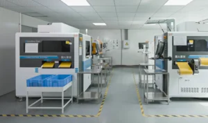
When you work with a partner who maintains complete manufacturing control—operating their own dedicated workshops with advanced equipment rather than brokering work to unknown facilities—you gain consistency, traceability, and accountability. You’re not wondering which factory actually produced your boards or whether quality standards were truly met. Everything happens under one roof with one team responsible for your success.
Certifications matter, but they’re just the baseline. ISO 9001 quality management, ISO 13485 medical device standards, IATF 16949 automotive certification, and ISO 14001 environmental responsibility—these credentials demonstrate capability, but the real value comes from the systematic thinking they represent. A certified partner has documented processes, continuous improvement programs, and quality cultures that catch issues before they become problems.
The global reach combined with rapid responsiveness creates competitive advantage. Whether your team is in North America, Europe, Japan, or Southeast Asia, you need a partner who understands your market requirements, communicates clearly across time zones, and responds quickly to technical questions. The ability to turn prototypes in one week—or three days for emergency situations—can mean the difference between capturing a market opportunity and watching competitors move first.
Consider the comprehensive journey from concept to mass production. It begins with consulting services where experienced engineers help refine your design for optimal performance and manufacturability. Then comes rapid prototyping where you can test concepts quickly without committing to expensive tooling. Engineering stages involve iterative refinement based on testing results and manufacturing feedback. Finally, volume production scales up with consistent quality maintained through every unit.
For emerging technologies like eVTOL vehicles or AI-powered wearables, you need a manufacturing partner who understands not just how to build circuits today, but how to prepare for tomorrow’s requirements. This means investing in R&D for next-generation capabilities—flexible heat dissipation channels for high-power applications, transparent circuits for augmented reality, and ultra-thin designs that push physical limits.
The environmental responsibility that comes with ISO 14001 certification reflects a forward-thinking approach that increasingly matters to customers and regulators. As electronics proliferate across industries, sustainable manufacturing practices—from material selection and process chemistry to waste management and energy efficiency—become competitive differentiators.
Conclusion: Building the Future Together
The electronics industry stands at an inflection point where innovation demands capabilities that didn’t exist five years ago. Electric vehicles require flexible circuits that withstand automotive environments. Medical devices need biocompatible materials and rigorous documentation. Aerospace applications demand ultimate reliability. Consumer electronics push for thinner, lighter, more capable designs. Every industry faces its own unique challenges, but they all share one common requirement: manufacturing partners who can execute sophisticated flexible PCB designs with unwavering quality.
Your next product innovation—whether it’s a life-saving medical device, a revolutionary EV system, or a cutting-edge consumer gadget—depends on choosing a manufacturing partner who brings more than just fabrication capability. You need a partner with two decades of experience translating designs into reality, comprehensive certifications ensuring regulatory compliance, and specialized expertise in your specific application.
At Flex Plus, we’ve built our reputation by pushing the boundaries of what flexible PCB technology can achieve. From ultra-thin double-sided boards just 25 micrometers thick to three-meter-long specialized circuits, from breakthrough COB integration to complete assembly services, we provide the complete manufacturing control and technical partnership that turns ambitious concepts into market-leading products.
The question isn’t whether flexible PCBs will power tomorrow’s innovations—they already are. The question is whether your manufacturing partner has the expertise, capabilities, and commitment to bring your vision to life with the quality and reliability your customers deserve. Because in today’s competitive landscape, your manufacturing partner isn’t just producing boards. They’re powering your innovation, enabling your success, and helping you build the future.