
Flexible printed circuit boards have revolutionized modern electronics by offering what rigid boards simply cannot—the ability to bend, fold, and adapt to complex three-dimensional spaces. Unlike traditional FR-4 rigid PCBs that occupy fixed rectangular footprints, flex PCBs conform to the product’s shape, dramatically reducing both space and weight. This adaptability has made them indispensable in today’s most demanding applications, from the smartwatch on your wrist to the life-saving medical implants monitoring patients’ hearts, and the sophisticated control systems powering electric vehicles.
The importance of flex PCBs extends beyond mere space savings. In wearable devices, they enable comfortable, body-conforming designs that users can wear all day without noticing. In medical equipment, they provide the biocompatibility and reliability necessary for devices that literally keep people alive. In electric vehicles, they withstand constant vibration, temperature fluctuations, and the demanding environment of automotive applications while maintaining signal integrity. However, achieving this level of performance requires meticulous attention to layout techniques that prevent the mechanical and electrical failures that have plagued poorly designed flexible circuits.

Material Selection: The Foundation of Reliable Flex PCB Design
The journey to a reliable flex PCB begins long before the first trace is routed—it starts with intelligent material selection. Traditional flex PCBs use adhesive-based polyimide laminates, where copper foil is bonded to the polyimide substrate using acrylic or epoxy adhesives. While this construction method has served the industry for decades, it introduces a critical weakness: the adhesive layer itself becomes a stress concentration point during repeated flexing.
Adhesiveless materials eliminate this vulnerability entirely. By using a special bonding process that fuses copper directly to the polyimide without intermediate adhesive layers, these advanced laminates significantly enhance mechanical reliability. The absence of adhesive means there’s no layer that can delaminate, crack, or fail under thermal cycling or mechanical stress. For applications requiring millions of flex cycles—think of a laptop hinge or a robotic arm joint—this difference translates directly into product longevity.
Beyond the base material, via design plays an equally crucial role in preventing failures. Standard through-hole vias with minimal annular rings create stress risers where the copper plating meets the substrate. Under flexing conditions, these stress points become crack initiation sites. Teardrop vias address this vulnerability by gradually transitioning from the trace width to the via pad, distributing stress over a larger area rather than concentrating it at sharp corners. Similarly, increasing annular ring size provides more copper-to-pad contact area, improving both mechanical strength and solderability while reducing the likelihood of pad pullaway during assembly or field use.
The choice between 25-micron and 50-micron polyimide thickness directly impacts both flexibility and durability. Thinner substrates bend more easily and can achieve tighter bend radii, making them ideal for compact wearable devices. However, they offer less mechanical support and may require additional reinforcement in high-stress areas. At Flex Plus (Xiamen) Co., Ltd, we’ve developed expertise in balancing these trade-offs, regularly producing ultra-thin double-sided flex PCBs with overall thicknesses as low as 25 microns while maintaining gold plating and long-term reliability.
Strategic Design Techniques for Enhanced Mechanical Integrity
Even with optimal materials, flex PCB layout requires design techniques that work with—rather than against—the material’s inherent properties. One of the most effective strategies involves incorporating stiffeners in critical areas where components mount or connectors attach. These rigid sections, typically made from FR-4 or polyimide, provide the dimensional stability necessary for reliable solder joints and connector mating while preserving flexibility elsewhere.
The art lies in strategic stiffener placement. Mounting a dense array of integrated circuits or a high-pin-count connector directly onto a flexible substrate invites reliability problems. The flexible material cannot provide adequate support during thermal cycling, potentially leading to solder joint failures or connector misalignment. By bonding stiffeners beneath these critical zones, designers create local “islands” of rigidity that handle mechanical stress without compromising the circuit’s overall flexibility. This hybrid approach has proven essential in smartphone flex PCBs, where cameras, processors, and connectors must remain stable despite the phone’s constant movement and temperature changes.
Routing techniques present another critical consideration for preventing signal degradation and mechanical failures. While rigid PCB designers routinely use 90-degree corners to conserve space, flex circuits demand a different approach. Sharp bends create stress concentration points where copper traces are most likely to crack during flexing. The solution involves designing smooth curved traces that distribute bending stress evenly across the conductor’s length. Think of it like bending a wire—gradual curves survive millions of cycles, while sharp kinks fail quickly.
Cross-hatched ground planes rather than solid copper pours offer another mechanical advantage in flex circuits. Solid copper planes resist bending, making the entire circuit stiffer and more prone to cracking at flex points. Cross-hatched patterns provide adequate electrical grounding while allowing the substrate to flex more naturally. The gaps between copper allow the polyimide to bend without fighting against a stiff copper sheet trying to maintain its shape.
Trace width and spacing require careful consideration beyond standard electrical requirements. Wider traces distribute current more evenly and resist cracking better than narrow ones, but they also increase stiffness. The optimal balance depends on the circuit’s flex requirements—dynamic flexing applications benefit from slightly narrower traces in flex zones, while static flex-to-install designs can use wider traces for enhanced current capacity and reliability.
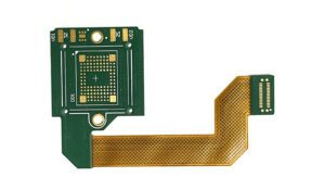
Transitioning to Rigid-Flex: When Flexibility Alone Isn’t Enough
While purely flexible circuits excel in many applications, some designs benefit from the strategic combination of rigid and flexible sections within a single board structure. Rigid-flex PCBs represent this evolution, integrating rigid board sections for component mounting with flexible interconnections that eliminate traditional connectors and cables.
This combination addresses several common engineering challenges simultaneously. First, it eliminates the connector reliability problems that plague many electronic assemblies. Every connector represents a potential failure point—pins can corrode, housings can crack, and contacts can lose their spring tension over time. By replacing connectors with flexible circuit sections, rigid-flex designs inherently improve long-term reliability. Second, they enable three-dimensional packaging strategies impossible with purely rigid or purely flexible circuits. The rigid sections provide stable mounting platforms while the flexible sections fold, wrap, or conform to fit within tight enclosures.
Consider a wearable fitness tracker. The main circuit board might contain the processor, memory, and display driver as a rigid section, while flexible arms extend out to connect sensors positioned around the user’s wrist. This configuration minimizes overall size, eliminates fragile connectors between sections, and allows the device to conform comfortably to varying wrist sizes. Without rigid-flex technology, achieving the same functionality would require multiple separate boards connected by cables or flex circuits, increasing assembly complexity and introducing multiple potential failure points.
In medical devices, rigid-flex technology proves even more critical. An implantable cardiac monitor might use a rigid section for the main electronics and battery, with flexible extensions reaching to electrode contact points. The rigid section provides the dimensional stability necessary for reliable battery contacts and integrated circuit mounting, while the flexible sections accommodate the movement of surrounding tissue without transmitting stress to delicate solder joints. This design approach has enabled a new generation of minimally invasive medical devices that improve patient outcomes while reducing surgical complexity.
Electric vehicles present perhaps the most demanding application environment for rigid-flex PCBs. Battery management systems must monitor dozens of individual cells spread throughout large battery packs, requiring circuits that can route signals across significant distances while withstanding constant vibration, temperature extremes from -40°C to 125°C, and potential exposure to moisture or chemicals. At Flex Plus, our IATF 16949 certification ensures that automotive-grade rigid-flex solutions meet these stringent requirements, delivering the reliability that EV manufacturers demand for safety-critical applications.
The layout techniques for rigid-flex circuits combine all the best practices of flexible circuit design with additional considerations for the rigid-to-flex transitions. These transition zones represent the highest-stress regions in the entire assembly—they’re where material properties change abruptly, and where mechanical stress concentrates during flexing. Designers must carefully control copper features in these zones, avoiding traces that run perpendicular to the bend line and ensuring adequate strain relief through careful trace routing and stiffener placement.
Stack-up symmetry becomes particularly important in rigid-flex designs. Asymmetric constructions—where copper or polyimide layers are unbalanced around the neutral axis—tend to warp, twist, or curl during manufacturing or thermal cycling. By maintaining symmetry wherever possible, designers ensure that thermal expansion forces balance out, keeping the circuit flat and preventing stress-induced failures. This principle applies equally to purely flexible circuits but becomes especially critical in rigid-flex designs where different material properties meet.
Designing for Dynamic vs. Static Flex Applications
Not all flexible circuits face the same mechanical demands. Understanding the distinction between dynamic and static flex applications fundamentally influences layout strategy. Dynamic flex circuits must withstand repeated bending throughout their service life—tens of thousands or even millions of cycles in applications like printer heads, robotic joints, or folding displays. These designs require the most careful attention to material selection, minimum bend radius, and trace routing to ensure adequate flex life.
Static flex-to-install applications, by contrast, bend only during product assembly and remain fixed thereafter. While they still benefit from flexible circuit construction—enabling three-dimensional routing and reducing connector count—they face less demanding mechanical requirements. Designers can use slightly thicker materials, tighter bend radii during assembly, and somewhat less conservative trace layouts since the circuit won’t experience repeated flexing in the field.
For dynamic applications, establishing appropriate minimum bend radius becomes critical. Generally, the minimum bend radius should be at least ten times the circuit’s total thickness for circuits that flex occasionally, and twenty times or more for circuits experiencing continuous flexing. A circuit with a 0.2mm total thickness, for example, should maintain at least a 4mm bend radius for dynamic applications. Violating these guidelines dramatically shortens flex life by introducing excessive strain into the copper conductors.
The flex zone itself requires special attention in dynamic applications. Designers typically avoid placing components, vias, or stiffeners within the active flex region, instead positioning them in static areas on either side of the bend. Traces should run perpendicular to the bend axis when crossing flex zones, as this orientation experiences less strain than traces running parallel to the bend. Where parallel routing is unavoidable, using multiple narrow traces rather than single wide ones helps distribute stress and reduce the likelihood of fatigue failures.
Conclusion: Engineering Excellence Enables Innovation
The sophisticated layout techniques discussed here—from adhesiveless materials and teardrop vias to strategic stiffener placement and rigid-flex integration—represent the accumulated knowledge of decades of flexible circuit evolution. They’re not merely best practices or suggestions; they’re essential requirements for preventing the mechanical and electrical failures that can compromise product reliability and user safety.
At Flex Plus (Xiamen) Co., Ltd, these techniques form the foundation of our engineering approach. Our 20+ years of flexible circuit manufacturing experience, combined with ISO 13485 certification for medical devices and IATF 16949 certification for automotive applications, ensures that every design we produce incorporates these proven reliability principles. Whether developing ultra-thin wearable circuits at 25 microns total thickness, biocompatible medical device flex PCBs, or automotive-grade rigid-flex solutions for electric vehicle applications, we apply the same rigorous attention to layout details that prevent failures in the field.
The transition from concept to reliable product requires more than just following design rules—it demands deep understanding of how materials behave under stress, how manufacturing processes affect final product characteristics, and how different application environments impose unique requirements on circuit design. Our engineering partnership approach provides comprehensive design support from initial concept through mass production, offering DFM analysis that identifies potential reliability issues before they become expensive problems.
As electronics continue evolving toward smaller, lighter, and more capable devices, flexible and rigid-flex circuits will play an increasingly critical role. The wearables, medical devices, and electric vehicles of tomorrow will demand even greater performance from their flexible interconnections—higher density, tighter bend radii, improved signal integrity, and longer service life. By mastering the layout techniques that prevent failures today, we prepare for the innovation challenges of tomorrow, enabling the next generation of electronic devices that improve lives and drive technological progress forward.
The path from a flexible circuit concept to a reliable, manufacturable product involves hundreds of detailed decisions about materials, layout, and process control. Each decision either contributes to or detracts from the final product’s reliability and performance. At Flex Plus, we’ve built our reputation on making those decisions correctly, delivering flexible PCB solutions that our customers depend on for their most demanding applications. Because in the end, layout techniques aren’t just about preventing failures—they’re about enabling innovation through superior flexible circuit solutions that perform reliably, year after year, in the real-world conditions that matter most.