
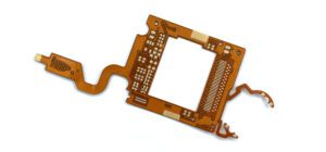
When you’re designing the next generation of electronics—whether it’s a foldable smartphone, a medical implant, or an electric vehicle display—one material choice stands out: Pyralux. This isn’t just another substrate option. It’s the foundation that determines whether your flexible PCB bends without breaking, withstands extreme temperatures, and delivers consistent electrical performance over thousands of cycles.
The challenge? Choosing the right thickness. Too thin, and you risk mechanical failure. Too thick, and you lose the flexibility that makes these circuits revolutionary. This decision isn’t just technical—it’s strategic. It affects your product’s reliability, manufacturing yield, and ultimately, your customer’s experience.
Pyralux has become the gold standard in flexible electronics for good reason. As a polyimide-based laminate system, it offers exceptional thermal stability, chemical resistance, and mechanical flexibility that rigid FR-4 boards simply cannot match. Industries ranging from aerospace to wearable technology depend on Pyralux to enable designs that were impossible just a decade ago.
But here’s what most engineers overlook: the thickness options available in Pyralux aren’t just about making things thinner or more robust. They’re about finding that precise balance point where flexibility meets durability, where performance meets manufacturability. Understanding these options transforms you from someone who specifies materials to someone who engineers solutions.
Understanding Pyralux Thickness Variations: A Deep Dive into Your Options
Pyralux laminates arrive in your design lab with an impressive range of configuration options. The polyimide dielectric layer—the heart of any flexible PCB—comes in thicknesses spanning from 12 micrometers (0.5 mils) up to 125 micrometers (5.0 mils), with specialty options reaching 150 micrometers (6.0 mils) and beyond for specific applications. This isn’t arbitrary. Each thickness increment represents a deliberate trade-off between flexibility and structural integrity.
Consider the thinnest options first. A 12-micrometer polyimide layer creates circuits so flexible they can wrap around a pencil without damage. These ultra-thin constructions find homes in applications where space is measured in fractions of millimeters—think about the flexible circuits inside your smartphone’s hinge mechanism or the connection between a wearable device’s sensor and its processor. The flexibility is extraordinary, but it comes with constraints. These thin substrates require careful handling during manufacturing and assembly. They’re more susceptible to tears during processing and demand precise registration control.
Moving up the thickness ladder, the 25-micrometer (1.0 mil) polyimide represents what many engineers consider the “sweet spot” for general flexible PCB applications. This thickness provides substantial flexibility—it can still bend through tight radiuses repeatedly—while offering enough structural support to handle standard SMT component assembly. Medical device manufacturers particularly favor this thickness range for implantable devices and diagnostic equipment where biocompatibility meets mechanical reliability.
When your application demands greater mechanical stability, the 50-micrometer (2.0 mil) and 75-micrometer (3.0 mil) options step forward. These thicker dielectrics substantially improve the circuit’s resistance to puncture and tearing. They can support heavier component loads without deformation and provide better dimensional stability during thermal cycling. Electric vehicle manufacturers frequently specify these thicknesses for dashboard displays, head-up display systems, and camera modules where the circuit experiences constant vibration and temperature fluctuations.
The copper foil thickness adds another critical dimension to your design equation. Pyralux systems offer copper ranging from 7 micrometers (¼ ounce) up to 70 micrometers (2 ounce), with even thicker options available for high-current applications. The copper type matters too—rolled annealed (RA) copper provides superior flexibility for dynamic flexing applications, while electrodeposited (ED) copper offers finer line width capabilities for high-density interconnect designs.
Here’s where it gets interesting: the total stack-up thickness dramatically affects your circuit’s flexural behavior. A single-layer flex PCB with 25-micrometer polyimide and 18-micrometer copper might measure just 0.1 millimeters total thickness. Double-sided constructions typically reach 0.32 millimeters. Multilayer rigid-flex combinations can exceed 0.42 millimeters, depending on the layer count and construction method.
But thickness isn’t just about the numbers—it’s about tolerance control. The dielectric thickness tolerance directly impacts your circuit’s electrical performance consistency. Variations in dielectric thickness create impedance fluctuations along transmission lines, causing signal integrity issues at high frequencies. Premium Pyralux materials maintain tight thickness tolerances, typically within ±5% for standard constructions. This precision becomes non-negotiable in telecommunications equipment, optical transceiver modules, and high-speed data transmission applications where signal loss and timing jitter cannot exceed strict specifications.
Temperature performance intersects with thickness selection in fascinating ways. Thicker polyimide layers generally provide better thermal mass and heat dissipation, helping protect sensitive components during temperature excursions. The Pyralux HT material system, for instance, offers the highest operating temperature rating available—maintaining dimensional stability and electrical performance well beyond standard polyimide grades. This becomes critical in automotive under-hood applications and industrial control systems where ambient temperatures regularly exceed 150°C.
Selecting the Right Thickness: A Strategic Framework for Your Application
Choosing the appropriate Pyralux thickness isn’t a one-size-fits-all decision. It requires understanding your application’s unique mechanical demands, environmental conditions, and performance requirements. Our comprehensive flexible PCB design rules guide provides essential parameters for successful implementation. Let’s break down this selection process into a practical framework you can apply to your next project.
Start with flexibility requirements. How many flex cycles will your circuit endure? Will it bend dynamically during use or remain in a static bent configuration? A camera module in an automotive mirror that articulates thousands of times daily demands different considerations than a one-time installation flex in consumer electronics. For dynamic flexing applications—particularly those exceeding 100,000 cycles—thinner polyimide substrates with rolled annealed copper offer superior fatigue resistance. The thinner material experiences less stress on the outer fibers during bending, extending flex life dramatically.
The bend radius calculation provides quantitative guidance here. Industry standards suggest minimum bend radii of 6 to 10 times the total material thickness for one-time bends, and 20 to 50 times thickness for dynamic flexing applications. If your design requires a 3-millimeter bend radius with dynamic flexing, you’re looking at maximum total thickness around 0.15 millimeters—pointing you toward thinner polyimide options.
Mechanical load capacity forms your second consideration pillar. Will the flex circuit support connectors? Heavy components like inductors or transformers? Each component adds mechanical stress to the substrate. Thicker polyimide constructions provide superior tensile strength and tear resistance, essential when flex PCBs act as structural elements rather than purely interconnect solutions. In applications like smart helmets for F1 racing or mining equipment, where the circuit board must withstand significant mechanical shock and vibration, the 50 to 75-micrometer polyimide range offers the necessary durability without sacrificing flexibility entirely.
Environmental conditions introduce another critical variable. Temperature extremes, humidity exposure, chemical contact—each environmental factor influences your thickness selection. Aerospace and defense applications operating across temperature ranges from -55°C to +200°C benefit from thicker polyimide constructions that maintain dimensional stability through extreme thermal cycling. The additional material mass reduces coefficient of thermal expansion mismatch stresses between the circuit and rigid sections in rigid-flex designs.
For medical device applications, particularly those involving biocompatible requirements and sterilization processes, thickness selection intersects with regulatory compliance. ISO 13485-certified manufacturing processes demand consistent thickness control to ensure reproducible electrical and mechanical performance. Medical implantables typically favor thinner constructions (25 micrometers or less) to minimize device profile, while external diagnostic equipment can leverage thicker substrates for enhanced durability during repeated sterilization cycles.
The electric vehicle industry presents particularly demanding thickness selection challenges. Consider an EV’s head-up display system: the flexible interconnect must survive 150°C temperature spikes under direct sunlight, withstand vibration across the vehicle’s operational spectrum, and maintain signal integrity for high-resolution video transmission. This application typically requires 50-micrometer polyimide with controlled impedance design, providing the thermal stability and mechanical robustness necessary for automotive service life expectations exceeding 15 years.
Telecommunications and optical transceiver applications shift the selection criteria toward electrical performance. Here, dielectric thickness tolerance and material loss tangent become paramount. High-frequency signal transmission demands tight impedance control—typically ±10% or better—requiring precision thickness control and low-loss dielectric materials. The Pyralux AP series, specifically engineered for these applications, offers exceptional dimensional stability and low dielectric loss even at millimeter-wave frequencies.
Manufacturing considerations also factor into thickness selection, though designers often overlook this aspect. Thinner polyimide substrates require specialized handling equipment and process controls to prevent material damage during fabrication. They’re more susceptible to processing defects like wrinkles, tears, and registration errors. If you’re targeting aggressive production schedules or high-volume manufacturing, slightly thicker constructions (25 to 50 micrometers) often improve manufacturing yield and reduce production costs despite the material price premium.
The emerging low-altitude airspace industry—encompassing drones, eVTOL vehicles, and air taxis—introduces unique thickness selection requirements. These applications demand extreme weight optimization while maintaining flight-critical reliability. Ultra-thin Pyralux constructions enable significant weight reduction across thousands of circuit boards in a single vehicle. However, the circuits must also withstand vibration, electromagnetic interference, and environmental exposure throughout their operational envelope. This typically drives designs toward 25-micrometer polyimide with specialized RA copper and controlled impedance design.
Beauty tech applications offer an interesting counterpoint. Tech-driven beauty gadgets prioritize user experience—they must feel comfortable against skin, fold into compact storage configurations, and survive repeated mechanical stress from daily use. These consumer products typically favor thinner polyimide constructions (12 to 25 micrometers) that enable tight bend radii and minimize device profile, even though the circuits don’t face extreme environmental conditions or long service life requirements.
Augmented reality wearables and AI glasses present perhaps the most demanding thickness selection challenges. These devices require ultra-thin, ultra-light circuits that conform to complex three-dimensional shapes while supporting high-speed data transmission for real-time image processing. The flexible PCBs often integrate optical components, requiring precise dimensional control and planarity. This application space pushes toward the thinnest available Pyralux options while demanding premium thickness tolerances and specialized assembly processes.
The Flex Plus Advantage: Engineering Excellence in Flexible PCB Solutions
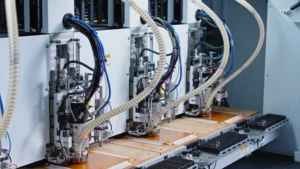
At Flex Plus (Xiamen) Co., Ltd, we’ve spent over 20 years perfecting the art and science of flexible PCB manufacturing. Our experience with Pyralux thickness selection goes far beyond simply reading datasheets—it comes from manufacturing thousands of flexible circuits across industries and learning what actually works in production and field deployment.
When you partner with Flex Plus, you’re not just getting a PCB fabricator—you’re accessing engineering expertise that spans from concept development through mass production. Our design-for-manufacturability analysis specifically addresses thickness selection, helping you avoid costly mistakes before they reach the fabrication stage. We’ve seen too many beautiful designs fail in manufacturing because thickness tolerances weren’t properly specified or because the selected construction couldn’t survive assembly processes.
Our certification portfolio reflects our commitment to quality across diverse industries. ISO 9001 certification ensures consistent quality management systems. ISO 13485 certification validates our medical device manufacturing capabilities, critical for biomedical-compatible flexible PCBs where thickness control directly impacts device performance and regulatory compliance. IATF 16949 certification demonstrates our automotive industry expertise, particularly relevant for EV manufacturers requiring flexible circuits that survive harsh under-hood environments and maintain performance across vehicle service life.
What sets Flex Plus apart is our complete manufacturing control. Unlike brokers or trading companies, we operate dedicated 8,000+ square meter production facilities equipped with advanced processing equipment specifically configured for Pyralux materials. This means we control every aspect of fabrication—from incoming material inspection through final electrical testing. We maintain in-house expertise in handling ultra-thin polyimide constructions, tight tolerance multilayer lamination, and controlled impedance design.
Our breakthrough flexible COB (Chip-on-Board) technology represents the next evolution in flexible electronics integration. By combining industry-leading die bonding precision (wafer offset angle tolerance within ±5°) with innovative magnetic fixture technology, we solve challenges that make competing manufacturers struggle. Our micron-level precision packaging achieves COB and encapsulation thickness tolerances of 50-100 micrometers (±25-50 micrometers), with ultra-fine dam processes reaching ±5-micrometer thickness control. This level of precision enables ultra-thin electronic modules that push beyond traditional packaging capabilities.
The practical benefits for your project are substantial. Consider a medical device requiring flexible substrate COB integration: we can deliver complete assemblies with total thickness under 200 micrometers, including the chip, encapsulation, and flexible substrate. This level of integration eliminates multiple assembly steps, reduces connection points (improving reliability), and maintains flexibility characteristics throughout the assembly. It’s innovation that transforms product possibilities.
Our specialized capabilities extend to long flexible PCBs—up to 3 meters in length—essential for industrial automation systems, telecommunications infrastructure, and specialized automotive applications. We maintain expertise across single-layer constructions through complex multilayer rigid-flex boards, handling copper thicknesses from 7 micrometers for fine-line applications up to 70 micrometers for high-current requirements.
Fast turnaround capabilities support your aggressive development schedules. We offer rapid prototyping services with standard delivery within one week and emergency turnaround in three days when your timeline demands it. This quick-turn capability doesn’t compromise quality—every prototype receives the same rigorous inspection and testing as production volumes, helping you identify and resolve design issues early in your development cycle.
Our global customer base spanning North America, South America, Europe, Japan, Taiwan, and Southeast Asia demonstrates the universal applicability of our Pyralux thickness selection expertise. Whether you’re developing next-generation AR wearables in Silicon Valley, automotive camera systems in Germany, medical diagnostic equipment in Japan, or telecommunications infrastructure in Taiwan, our engineering team brings relevant industry experience to your project discussions.
The philosophy driving Flex Plus centers on partnership rather than transaction. We engage with your engineering team early in the design process, offering material consultation, thickness recommendations, and DFM feedback that reduces technical risk and optimizes manufacturing yield. This collaborative approach has helped over 2,500 customers successfully launch products across industries where flexible PCB performance directly impacts product differentiation and customer satisfaction.
Looking ahead, the flexible electronics industry continues pushing toward thinner, more complex constructions that challenge traditional manufacturing capabilities. Emerging applications in low-altitude airspace, beauty tech innovation, and augmented reality demand flexible PCBs that seemed impossible just five years ago. At Flex Plus, we’re investing in next-generation capabilities—advanced materials like TPU circuits offering stretchability and biocompatibility, transparent PCB technologies, and specialized heat dissipation solutions integrated into ultra-thin flexible substrates.
Understanding Pyralux thickness options represents more than technical knowledge—it’s strategic intelligence that influences your product’s competitiveness, manufacturing efficiency, and field reliability. The right thickness selection balances flexibility and durability in ways that enable your innovation while ensuring production success. Whether you’re engineering the next breakthrough in electric vehicles, medical devices, telecommunications, or consumer electronics, that selection deserves careful consideration supported by manufacturing expertise.
At Flex Plus, we believe every flexible PCB project deserves the precision, reliability, and innovation that comes from true manufacturing excellence. From initial concept discussions through volume production, we deliver flexible circuit solutions that empower your technological advancement while maintaining the certified quality standards your applications demand. Because in flexible electronics, the difference between good enough and exceptional often comes down to choosing the right thickness—and knowing how to manufacture it consistently.