
In the world of modern electronics, reliability isn’t just a feature—it’s everything. When a flexible PCB fails in an electric vehicle’s head-up display system at highway speeds, or a medical device malfunctions during a critical procedure, or a drone’s control circuit breaks mid-flight, the consequences extend far beyond simple product returns—compromising safety, damaging brand reputation, and triggering costly recalls.
Flex PCBs have become the backbone of innovation across industries that demand both performance and reliability. From IATF 16949-certified automotive electronics in electric vehicles to ISO 13485-compliant biomedical devices, from precision smartphone modules to augmented reality wearables, flexible circuits enable designs that would be impossible with traditional rigid boards. Yet this versatility comes with a critical requirement: flawless design execution. A single oversight in flex PCB design can cascade into catastrophic field failures, undermining months of development work and millions in investment.
The challenge lies in understanding that flexible PCBs aren’t simply bendable versions of rigid boards. They operate under entirely different mechanical, electrical, and thermal stresses. Understanding fundamental flexible PCB design rules becomes essential for any engineer transitioning from rigid to flexible circuit design. Engineers transitioning from rigid PCB design often carry assumptions that don’t translate to flexible substrates, leading to preventable failures. This article examines five critical mistakes that commonly destroy flex PCB reliability and provides practical guidance to avoid them—insights drawn from over two decades of manufacturing experience serving demanding industries across North America, Europe, and Asia.
Mistake #1: Overlooking Bending Requirements and Material Selection
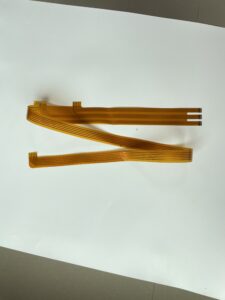
The most fundamental error in flex PCB design stems from inadequate analysis of how the circuit will actually bend in its final application. Many designers specify a flex PCB without thoroughly documenting bend radius, frequency of flexing, and the type of movement required—whether static (bent once during assembly), dynamic (occasional flexing during use), or continuous flex (constant movement like in a printer head).
This oversight becomes catastrophic when paired with inappropriate material selection. Polyimide substrates come in various grades, each engineered for specific applications. Standard polyimide works well for static applications, but dynamic flexing requires specialized materials with enhanced elongation properties. Copper foil selection matters equally—rolled annealed copper offers superior flexibility compared to electrodeposited copper, bending up to 100,000 cycles in properly designed circuits versus potential failure after just hundreds of cycles with the wrong material.
Consider a real-world example from the wearable technology sector: An AR glasses manufacturer specified a standard flex PCB for the temple connection without accounting for the repeated bending that occurs every time users put on or remove the glasses. Within weeks of market launch, field returns spiked due to cracked traces. The root cause? Standard electrodeposited copper with a minimum bend radius specification that didn’t match the actual use case. Switching to rolled annealed copper and redesigning the bend geometry resolved the issue, but not before significant reputation damage and warranty costs.
The critical lesson: Begin every flex PCB design by mapping actual bending scenarios. Document minimum bend radius requirements—typically at least ten times the total thickness for dynamic applications. IPC-2223 standards provide detailed testing protocols for validating flex circuit mechanical performance under various bending conditions. Select materials that match your application profile. For medical devices requiring biocompatible solutions or EV applications demanding IATF 16949 compliance, material selection becomes even more critical, as these must meet both mechanical performance and regulatory requirements.
Mistake #2: Improper Stack-up Configuration
Stack-up design represents the structural foundation of any flex PCB, yet it’s frequently treated as an afterthought rather than a strategic decision. The arrangement of copper layers, dielectric materials, and coverlay determines not only electrical performance but also mechanical reliability, especially in bend regions.
A common mistake involves symmetrical stack-ups in dynamic flex applications without considering neutral axis positioning. When a flex PCB bends, the outer layers experience tensile stress while inner layers face compression. The neutral axis—where stress approaches zero—should ideally align with your critical signal traces. In a single-layer design, traces sit at maximum stress. Adding balanced layers above and below can position traces closer to the neutral axis, dramatically improving fatigue resistance.
Another critical error involves inconsistent dielectric thickness across flexible and rigid sections. Abrupt thickness transitions create stress concentration points that initiate delamination failures. In industrial control systems operating in high-vibration environments, these stress risers become failure modes. The solution requires gradual thickness transitions and strategic stiffener placement to distribute mechanical loads.
Layer count decisions also impact reliability more than designers typically recognize. While adding layers increases design complexity and cost, sometimes moving from a two-layer to a four-layer design with better neutral axis positioning proves more reliable and ultimately more cost-effective than fighting yield issues and field failures. Telecommunications equipment manufacturers have learned this lesson when deploying optical transceiver modules—the initial premium for additional layers pays dividends in reduced failure rates over the product’s operational lifetime.
Material selection within the stack-up extends beyond the base polyimide. Adhesive choice matters significantly. Adhesiveless constructions offer superior flexibility and thermal performance for high-reliability applications like aerospace electronics, where every potential failure mode must be eliminated. However, they require more sophisticated manufacturing capabilities and higher upfront costs. Understanding these trade-offs allows informed decisions aligned with your application’s criticality and budget constraints.
Mistake #3: Strategic Placement Failures and Stress Point Creation
How you position copper features within your flex PCB can mean the difference between a circuit that survives millions of flex cycles and one that fails in field testing. Yet many designs inadvertently create stress concentration points through poor trace routing, via placement, and component positioning decisions.
Sharp angles represent the most notorious culprits. Traces routed at 90-degree angles in flex regions create stress risers that initiate cracks under repeated bending. Following proper flex circuit design guidelines helps engineers avoid these common trace routing errors from the outset. The copper literally tears at these corners as mechanical stress concentrates. The solution sounds simple—use curved traces or 45-degree angles—but implementing this consistently across complex designs requires discipline and proper design rule checking.
Via placement in bend regions creates another common failure mode. Vias represent discontinuities in the flexible substrate structure, creating rigid points that disrupt smooth bending motion. When vias must exist near flex zones, strategic placement becomes critical: Position them at bend radii where stress is minimized, never at the apex of the bend. For dynamic flex applications in precision smartphone modules or beauty tech gadgets requiring constant manipulation, the general rule is to keep vias completely out of flex regions whenever physically possible.
Component placement near flex zones requires equally careful consideration. Heavy components create mass loading that amplifies stress during flexing. A real example from the smart helmet industry illustrates this: An F1 racing helmet design placed a connector directly adjacent to a flex region connecting the rigid display board to the flexible sensor array. The mass of the connector, combined with vibration during high-speed racing, created fatigue failures. Repositioning the connector further from the flex zone and adding a strain relief feature eliminated the problem.
Trace staggering in multilayer flex designs provides another reliability enhancement often overlooked. When copper traces in different layers align vertically, they create a rigid column that resists bending. Offsetting traces between layers—a technique called staggering—maintains flexibility while providing necessary routing density. This proves particularly valuable in medical devices where miniaturization demands high trace density without compromising the flexibility required for biocompatible wearable sensors.
The pad-to-trace transition deserves special attention. Abrupt width changes create stress concentration points. Teardrop shapes at pad entrances gradually transition from narrow traces to wide pads, distributing stress more evenly. While teardrops add minimal cost and complexity, they significantly improve reliability in dynamic applications like drone control circuits and eVTOL vehicle electronics where vibration and movement are constant operational conditions.

Mistake #4: Routing Considerations and Cost-Performance Balance
Intelligent routing strategy separates reliable flex PCBs from problematic ones, yet many designers approach routing with rigid PCB mindsets. The fundamental difference: flex PCBs bend in three dimensions, and your routing strategy must account for how traces behave under mechanical deformation while balancing performance against manufacturing costs.
Trace width consistency in flex regions directly impacts reliability. While it’s tempting to minimize trace widths to maximize routing density, excessively thin traces in dynamic flex zones become vulnerable to fatigue failure. The industry guideline suggests minimum trace widths of 0.15mm for dynamic flex applications, though specific applications may require wider traces. For high-current applications in EV charging systems or power distribution circuits, wider traces become mandatory, but these wider traces must route around flex zones rather than through them.
Parallel trace routing creates another subtle failure mode. When multiple traces run in parallel through a flex region, they form a rigid strip that resists bending. Staggering parallel traces or routing them at slight angles to each other maintains better flexibility. This technique proves essential in telecommunications equipment where dense signal routing must coexist with mechanical flexibility requirements.
The balance between design complexity and manufacturing cost demands careful consideration. Every layer adds cost—not just in materials but in manufacturing complexity, yield impact, and testing requirements. A six-layer rigid-flex design might technically satisfy all requirements, but if a four-layer design with strategic routing achieves 95% of the performance at 60% of the cost, the latter often represents the better engineering decision. This becomes particularly relevant for consumer electronics and smartphone modules where market pressure demands cost optimization without compromising reliability.
Impedance control in flexible circuits introduces additional routing complexity. High-speed signals require controlled impedance, typically 50 or 100 ohms differential. Achieving this in flexible substrates where dielectric constants may vary from rigid sections requires careful stack-up design and trace geometry calculations. For precision applications like optical transceivers or AR wearables, impedance discontinuities at flex-to-rigid transitions can degrade signal integrity. Advanced simulation tools become essential for these designs, validating impedance profiles across the entire signal path.
Ground plane strategy in flex circuits differs significantly from rigid boards. Solid ground planes in flex regions create rigidity and cracking risk. Hatched or crosshatch ground planes maintain electrical performance while preserving flexibility. The hatch pattern density must balance EMI shielding effectiveness against mechanical flexibility—typically 50-70% copper coverage provides optimal compromise for dynamic flex applications.
Mistake #5: Inadequate Testing and Validation Protocols
The final critical mistake occurs not in design but in validation—or rather, the lack of comprehensive testing that simulates actual operating conditions. Many flex PCB projects proceed from prototype to production with only basic electrical testing, missing mechanical reliability validation that would expose design weaknesses before costly mass production.
Dynamic flex testing should mirror actual application conditions. If your device bends 50 times daily over a ten-year lifespan, your test protocol should simulate 180,000+ flex cycles at the specified bend radius. Automotive quality standards like IATF 16949 mandate comprehensive reliability testing that validates both electrical performance and mechanical durability under real-world conditions. Accelerated life testing under elevated temperatures or increased flex frequency can compress testing timelines while revealing potential failure modes. This level of validation is non-negotiable for medical devices requiring ISO 13485 compliance or automotive electronics under IATF 16949 certification, where regulatory requirements mandate comprehensive reliability testing.
Thermal cycling adds another validation dimension frequently overlooked. Temperature variations cause differential expansion between materials. A flex PCB that performs flawlessly at room temperature may fail under the thermal cycling experienced in industrial control systems (-40°C to +85°C) or automotive applications (-55°C to +125°C). Combined environmental testing—simultaneous temperature cycling and mechanical flexing—reveals failure modes that single-parameter testing misses.
Advanced inspection techniques provide early failure detection. High-resolution microscopy can identify early-stage crack propagation in copper traces before electrical failure occurs. X-ray inspection reveals internal defects in multilayer constructions and via formation. Time-domain reflectometry (TDR) characterizes impedance profiles across flex-to-rigid transitions. These tools transform quality assurance from reactive failure analysis to proactive defect prevention.
Design for testability represents another often-neglected consideration. Test points positioned for easy access during assembly validation, integrated current-sensing features for functional testing, and diagnostic circuits that enable field troubleshooting all contribute to long-term reliability and serviceability. For complex assemblies like aerospace electronics or military applications, built-in self-test capabilities can detect degradation before it impacts mission-critical functions.
Statistical process control during manufacturing provides the foundation for consistent quality. Even perfectly designed flex PCBs fail if manufacturing processes drift out of specification. Tracking key parameters—copper plating thickness, lamination pressure and temperature, coverlay registration accuracy—enables early detection of process variations before they impact reliability. Leading manufacturers implement real-time monitoring with automated feedback control, ensuring every production run meets the same exacting standards that validated prototypes achieved.
Building Reliability into Every Design
Flex PCB reliability doesn’t emerge from a single decision but from systematic attention to mechanical, electrical, and manufacturing considerations throughout the design process. The five critical mistakes outlined here—overlooking bending requirements, improper stack-up, stress point creation, inadequate routing strategy, and insufficient testing—represent the most common paths to failure, yet all are preventable through informed design choices and rigorous validation.
Success in flex PCB design requires partnership between design engineering, manufacturing expertise, and application knowledge. Understanding how your circuit will be used, how it will bend, what environmental stresses it faces, and what reliability standards it must meet forms the foundation for every technical decision. Materials selection, stack-up configuration, routing strategy, and validation protocols should all trace back to these fundamental application requirements.
The complexity of modern flex PCB applications—from ultra-thin beauty tech gadgets to mission-critical aerospace systems—demands manufacturing partners with deep technical expertise and comprehensive certifications. ISO 9001, ISO 13485, and IATF 16949 certifications aren’t simply regulatory checkboxes; they represent systematic quality management that turns design intent into consistent manufacturing reality. Advanced capabilities like flexible substrate COB integration, ultra-thin designs approaching 25 microns total thickness, and long-format processing up to three meters enable next-generation product innovations.
Real manufacturing expertise makes the difference between prototype success and production reliability. Comprehensive engineering support—DFM analysis, material consultation, stack-up optimization, and testing protocol development—transforms initial concepts into field-proven products. When your application demands never-fail reliability, whether serving millions of consumers or protecting critical infrastructure, manufacturing partnership becomes as important as design excellence.
Flex PCB design challenges will only intensify as applications push boundaries in miniaturization, performance, and environmental extremes. Electric vehicles demand higher power density and thermal performance. Medical devices require biocompatibility and surgical-grade reliability. Low-altitude airspace innovations like eVTOL vehicles and delivery drones need robust circuits that withstand constant vibration and thermal cycling. Meeting these challenges requires not just avoiding mistakes but embracing best practices that build reliability into every design decision.
The path from concept to reliable product isn’t always straightforward, but with proper attention to mechanical design fundamentals, strategic material selection, intelligent routing, and comprehensive validation, flex PCBs can deliver exceptional reliability even in the most demanding applications. By learning from common mistakes and implementing proven design strategies, engineers can create flexible circuits that don’t just meet specifications but exceed expectations across entire product lifecycles. In an era where electronics enable life-saving medical devices, electrify transportation, and connect billions of people, reliability isn’t optional—it’s the foundation upon which innovation builds.