
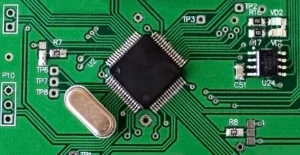
In today’s rapidly evolving electronics landscape, high-density interconnect (HDI) flex circuits have become essential components powering innovation across industries. From ultra-compact medical devices to sophisticated electric vehicle systems, these flexible marvels enable engineers to pack more functionality into increasingly smaller spaces. However, the success of any HDI flex circuit design hinges on understanding and implementing specific design parameters that can make or break your project.
As miniaturization trends continue to accelerate, mastering HDI flex circuit design rules has become non-negotiable for engineers pushing the boundaries of what’s possible in electronic design. Let’s explore the five critical parameters that demand your attention when developing high-density flexible PCB solutions.
The Critical Role of HDI Flex Circuits in Modern Electronics
High-density interconnect flex circuits represent the cutting edge of electronic design, offering unprecedented advantages in terms of size, weight, and performance. These advanced circuits feature finer lines, smaller vias, and higher connection density than traditional PCBs, enabling next-generation products that were previously impossible to manufacture.
The significance of HDI flex circuits spans numerous high-growth industries:
– Electric Vehicles: HDI flex circuits are vital components in EV systems including Head-Up Displays, wing mirrors, side CMS cameras, Lidar systems, and parking sensors, where reliability under harsh conditions is non-negotiable.
– Medical Devices: Biomedical-compatible HDI flex PCBs power life-saving equipment where miniaturization and flexibility meet stringent reliability requirements, particularly in implantable and wearable medical technologies.
– Telecommunications: The backbone of 5G infrastructure relies on HDI flex circuits to achieve higher data transmission rates in compact equipment designs.
– Aerospace Applications: From drones to eVTOL vehicles and air taxis, low-altitude airspace innovations depend on lightweight, reliable HDI flex solutions.
– Consumer Electronics: Smartphones, AR wearables, and AI glasses utilize HDI flex circuits to achieve thinner, lighter designs with enhanced functionality.
According to industry data, HDI technology enables size reductions of up to 40% compared to conventional designs while improving signal integrity and reducing electromagnetic interference. However, these benefits can only be realized when proper design rules are followed.
Parameter #1: IPC Standards Compliance – Your Quality Foundation
Adhering to industry standards isn’t just a box-checking exercise—it’s the foundation of reliable HDI flex circuit manufacturing. For high-density flexible PCBs, compliance with specific IPC standards is essential for ensuring quality, performance, and reliability. IPC standards provide critical guidance for manufacturers and designers alike.
The most relevant standards for HDI flex circuit design include:
IPC-6013: The Flexible Circuit Bible
This cornerstone standard outlines qualification and performance specifications specifically for flexible printed boards. It defines three product classes based on reliability requirements:
– Class 1: General Electronic Products
– Class 2: Dedicated Service Electronic Products
– Class 3: High-Reliability Electronic Products
For critical applications in medical devices, aerospace, or automotive systems, Class 3 compliance is often mandatory. As a certified flexible PCB manufacturer, Flex Plus ensures strict adherence to IPC-6013 requirements, particularly for high-reliability applications.
IPC-2223: Sectional Design Standard for Flexible Printed Boards
This standard provides essential guidance on flex-specific design considerations including:
– Materials selection
– Dimensional tolerances
– Layer stackup recommendations
– Bend area specifications
IPC-2226: Design Standard for High-Density Interconnect (HDI) Printed Boards
This critical standard specifically addresses HDI design requirements, covering:
– Microvia formation and reliability
– Sequential build-up technologies
– Material selection criteria for HDI applications
– Layout recommendations for optimal signal integrity
“Following IPC standards isn’t optional for high-reliability HDI flex circuits,” notes a senior engineer at Flex Plus. “These standards incorporate decades of industry knowledge and best practices that directly impact manufacturing yield and long-term reliability.”
Beyond compliance, working with a manufacturer certified to international quality standards like ISO 9001, ISO 13485 for medical applications, and IATF 16949 for automotive projects provides additional quality assurance. Flex Plus maintains these certifications, ensuring consistent manufacturing excellence across diverse industry requirements.
Parameter #2: Bending Requirements and Material Selection
Perhaps the most defining characteristic of flexible circuits is their ability to bend—whether in a single-time installation fold or for dynamic, repeated flexing during operation. The interplay between bending requirements and material selection represents one of the most critical design decisions in HDI flex circuit development.
Determining Minimum Bend Radius
According to IPC-2223, minimum bend radius calculations must account for:
1. Circuit Construction Type: Single-sided flex circuits can typically achieve tighter bend radii than double-sided or multilayer designs.
2. Material Thickness: As total thickness increases, the minimum bend radius must increase proportionally.
3. Copper Type and Thickness: Rolled annealed copper offers superior flex durability compared to electrodeposited copper, especially for dynamic flex applications.
The general rules for minimum bend radius are:
– Single/double-layer flex: ≥6× the material thickness
– Multilayer flex: ≥12× the material thickness
– Dynamic flexing applications: ≥20× the material thickness
For a typical single-layer flex circuit with 1 oz copper and standard polyimide, this translates to a minimum bend radius of approximately 0.6mm for single-flex applications and 2mm for dynamic flexing.
Strategic Material Selection
Material selection directly impacts both mechanical flexibility and electrical performance:
Base Materials:
– Polyimide (PI): The gold standard for flex circuits, offering excellent temperature resistance (up to 260°C) and dimensional stability
– Liquid Crystal Polymer (LCP): Superior electrical properties for high-frequency applications
– TPU (Thermoplastic Polyurethane): Provides stretchability for wearable applications
Copper Foil Options:
– Rolled Annealed Copper: Provides superior flex life (10× better than ED copper) due to grain structure aligned with rolling direction
– Electrodeposited (ED) Copper: More economical but limited flex life
– Copper Thickness: 18μm (1/2 oz) to 70μm (2 oz) depending on current requirements and flex needs
Adhesive Systems:
– Adhesiveless: Thinner overall stack-up with superior thermal performance
– Adhesive-Based: More economical with adequate performance for most applications
“The interaction between material selection and bending requirements can’t be overlooked,” emphasizes the engineering team at Flex Plus. “We’ve seen too many designs fail because material properties weren’t aligned with the mechanical requirements of the application.”
For dynamic flexing applications like foldable displays or continuously moving medical devices, specialized testing under IPC-TM-650 Method 2.4.3 should be performed to validate flexural endurance.
Parameter #3: Trace Routing and Geometry in Flex Regions
When designing HDI flex circuits, how you route traces—particularly in bend areas—can mean the difference between a reliable product and field failures. High-density designs push the limits of trace width and spacing, making proper routing even more critical.
Trace Orientation in Flex Regions
The cardinal rule for trace routing in flex areas is simple but frequently overlooked: traces should cross bend lines perpendicularly (at 90° angles) whenever possible. This orientation distributes stress evenly across the trace width rather than concentrating it along one edge, which would occur with traces parallel to the bend line.
For HDI applications where space constraints make perpendicular routing impossible, the minimum angle should not be less than 45° relative to the bend line.
Trace Geometry Considerations
HDI flex circuits can achieve much finer line width/spacing than conventional designs—typically down to 2/2mil (50μm/50μm) or even 1/1mil (25μm/25μm) in advanced applications. However, several geometry factors require careful attention:
1. Trace Width Consistency: Avoid abrupt changes in trace width, particularly in flex areas. Transitions should be gradual with a maximum 3:1 ratio.
2. Teardrop Reinforcement: Use teardrop-shaped reinforcement at all trace-to-pad and trace-to-via connections to prevent stress concentration points.
3. Hatched Ground Planes: Solid copper planes in flex regions should be avoided as they significantly increase stiffness. Instead, use crosshatched ground planes (typically 50-70% copper removal) in flex areas while maintaining solid planes in rigid regions.
4. Conductor Spacing in Flex Regions: Increase minimum spacing between conductors in flex areas by at least 30% compared to rigid areas to accommodate material deformation during bending.
According to industry data, properly designed trace geometry can increase flex life by 300-500% compared to non-optimized designs.
“In high-reliability applications like medical devices or aerospace systems, every detail of trace geometry matters,” notes a Flex Plus senior design engineer. “We’ve developed specialized design rules based on decades of manufacturing experience that go beyond basic IPC guidelines to ensure maximum reliability.”
Parameter #4: Layer Stackup and Via Strategy
HDI flex circuits achieve their remarkable density through sophisticated layer stackups and advanced via structures. Understanding the options and limitations is essential for successful high-density designs.
HDI-Specific Layer Stackups
HDI flex circuits typically utilize one of several standardized buildup sequences:
1. Type I: Single microvia layer on either top or bottom
2. Type II: Microvias on both top and bottom layers
3. Type III: Stacked microvias connecting multiple layers
4. Type IV: Staggered microvias with complex interconnections
Each type offers different tradeoffs between density, manufacturability, and cost. For the most advanced applications requiring maximum density, Type IV structures allow for the highest interconnection density but with increased manufacturing complexity.
For rigid-flex HDI designs, managing the transition between rigid and flex regions is particularly critical. The layer stackup must account for differences in material properties while maintaining consistent electrical characteristics.
Microvia Design Parameters
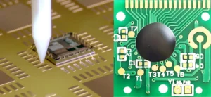
Microvias are the defining feature of HDI technology, with several critical design parameters:
1. Microvia Aspect Ratio: The ratio of depth to diameter should not exceed 1:1 for reliable laser drilling and plating.
2. Microvia Diameter: Typically ranges from 75μm to 150μm, with a minimum size determined by the capabilities of the manufacturer’s laser drilling equipment.
3. Capture Pad Size: Typically 100μm larger than the microvia diameter (50μm annular ring) to ensure reliable connection.
4. Microvia Placement: Microvias should not be placed in flex areas unless absolutely necessary. When required, they should be positioned at least 1mm away from the beginning of any bend region.
“The via strategy you choose fundamentally defines what’s possible with your HDI flex design,” explains a manufacturing engineer at Flex Plus. “Working closely with your manufacturer during the early design stages to understand their specific capabilities and design rules will save significant time and prevent costly redesigns.”
Parameter #5: Surface Finish and Final Plating Considerations
The surface finish selection for HDI flex circuits impacts not only solderability and contact resistance but also flexibility characteristics and long-term reliability.
Surface Finish Options for HDI Flex
Several surface finishes are commonly used for HDI flex circuits, each with specific advantages:
1. ENIG (Electroless Nickel Immersion Gold):
- Industry standard for high-reliability applications
- Excellent solderability and contact resistance
- Flat surface ideal for fine-pitch components
- Good shelf life (12+ months)
- Adds minimal thickness to the overall circuit
2. ENEPIG (Electroless Nickel Electroless Palladium Immersion Gold):
- Superior performance for both soldering and wire bonding
- Excellent for mixed-technology assemblies
- Preferred for flex COB (Chip-on-Board) applications
- Higher cost than standard ENIG
3. Immersion Tin:
- Economical option with good solderability
- Excellent for press-fit connections
- Limited shelf life (3-6 months)
- Not recommended for flex circuits that will undergo significant bending
4. Hard Gold (Electrolytic Gold):
- Superior wear resistance for connector applications
- Excellent for ZIF (Zero Insertion Force) connections
- Typically used selectively in specific areas rather than entire surface
For high-density applications requiring the ultimate in reliability, ENEPIG has become the preferred finish, particularly for advanced applications like flexible substrate COB integration where both solderability and wire bonding performance are critical.
Selective Plating Strategies
In sophisticated HDI flex designs, selective plating—applying different finishes to different areas of the same circuit—can optimize both performance and cost:
– Hard gold on contact areas for durability
– ENIG or ENEPIG on component mounting areas
– Bare copper with coverlay protection in flex areas
“The right surface finish selection requires balancing multiple factors including assembly method, environmental exposure, cost constraints, and flex requirements,” says a Flex Plus process engineer. “For critical applications like medical devices or aerospace systems, we typically recommend ENEPIG despite its higher cost due to its superior reliability characteristics.”
Conclusion
Successful HDI flex circuit design requires careful attention to these five critical parameters. By properly addressing IPC standards compliance, bending requirements and material selection, trace routing geometry, layer stackup and via strategy, and surface finish considerations, engineers can ensure their high-density projects achieve the perfect balance of miniaturization, reliability, and manufacturability.
As electronic devices continue to demand more functionality in smaller packages, mastering these HDI flex circuit design rules becomes increasingly important. Working with an experienced manufacturer like Flex Plus that specializes in advanced flexible PCB solutions can provide valuable guidance through the complex decision-making process.
With proper implementation of these five make-or-break parameters, your next HDI flex circuit project will be positioned for success, enabling the next generation of innovative electronic products across industries from medical devices and electric vehicles to aerospace applications and beyond.