
Ever wondered what makes your sleek smartphone so slim and your fitness tracker so, well… bendy? It’s not black magic (though it’s pretty close) – it’s the wizardry of flexible PCBs! These unsung heroes are the magical flying carpets of the electronics world, whisking our devices away to new realms of possibility while staying impossibly thin and bendable.
Prepare to have the curtain pulled back on one of electronics manufacturing’s most fascinating backstage performances. We’re about to expose the secrets behind flex PCB manufacturing – not because manufacturers are hiding anything, but because they’re too busy innovating while the rest of us are stuck with rigid desk jobs. (A fitting metaphor for non-flexible PCBs, wouldn’t you say?)
The Bendy Basics: What Makes a PCB Flex?
Before we dive into the manufacturing rabbit hole, let’s get familiar with these bendable beauties. Unlike their stiff, no-fun cousins (traditional rigid PCBs), flexible printed circuit boards are the yoga masters of the electronics world. They twist, they turn, they fold – all without throwing a tantrum or breaking a sweat.
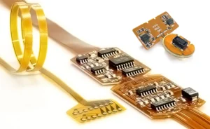
The secret sauce? Polyimide. This wonder material serves as the base substrate for most flexible PCB manufacturing processes. At just 12.5 to 125 microns thick (that’s thinner than a human hair having a really good flat-iron day), polyimide provides the perfect balance of flexibility and durability. It’s like that one friend who can touch their toes while also bench-pressing impressive weights – simultaneously flexible and strong.
On top of this magical polyimide layer, manufacturers add a thin copper foil (usually 18-70μm thick) through a lamination process that would make a sandwich artist jealous. This copper layer eventually becomes our circuit traces – the electronic roadways that make everything from your car’s dashboard display to your smart toothbrush actually work.
“But wait,” I hear you ask, “if these flexible PCBs are so bendy, how do they not snap the copper circuits?” Great question, hypothetical reader with excellent technical intuition! The copper used isn’t your everyday penny material – it’s special “RA copper” with elongated grain structures specifically designed to flex without fatigue. It’s basically copper that’s been to flexibility finishing school.
The Manufacturing Dance: Choreographing Circuits
Now, let’s peek behind the curtain at how these flexible wonders are actually made. Fair warning: there’s less dancing than promised, but plenty of fascinating precision steps.
The flexible PCB manufacturing process starts with what looks like a copper-polyimide sandwich. This material arrives in rolls or sheets at the factory, ready for its transformation from ordinary laminate to extraordinary circuit.
First step: cleaning. Because nothing ruins a good circuit like microscopic debris. This cleaning process is so thorough it would make your germaphobic aunt nod in approval. The material is scrubbed, rinsed, and prepped with more care than a priceless painting.
Next comes the most artistic part – circuit patterning. Unlike rigid PCBs where mechanical drilling is common, flexible PCB manufacturing often utilizes laser drilling for creating vias (those little holes that connect different layers). Why lasers? Because they’re precise, non-contact, and frankly, because lasers make everything cooler. It’s science.
Then comes the photolithography process – which sounds like something you’d study in art school but is actually a chemical process involving photoresist, UV exposure, and development. Think of it as taking a photo of the circuit design onto the copper. The unexposed photoresist washes away, leaving a protective mask in the exact shape of our desired circuits.
“The etching process is where the magic really happens,” explains a veteran Flex Plus engineer. “We’re essentially sculpting circuits with chemicals, removing unwanted copper while protecting the traces that will carry signals. It’s like creating microscopic copper rivers flowing through a polyimide landscape.”
After etching comes plating – where additional metal (usually gold or nickel) is added to the exposed copper traces. This isn’t just for bling factor (though it does look rather fancy) – it’s for protection and conductivity. Gold doesn’t tarnish, making it perfect for ensuring reliable connections over time.
What makes flexible PCB manufacturing particularly tricky is managing the tension between flexibility and durability. Too thin, and the circuit might not survive real-world use. Too thick, and it loses the flexibility that makes it special in the first place. It’s like trying to make the perfect crepe – too thick and it’s just a sad pancake, too thin and it tears when you look at it funny.
Applications: Where These Bendy Wonders Thrive
Now that we know how these flexible marvels are born, let’s talk about where they live out their bendy lives. Spoiler alert: they’re everywhere.
Electric vehicles might seem like the last place you’d expect flexibility, but modern EVs are packed with flexible PCBs. From the sleek displays on your dashboard to the sensors in your side mirrors and parking cameras, flexible circuits enable complex electronics to fit into increasingly streamlined designs. At Flex Plus, they’ve seen a surge in EV applications, with flexible PCBs appearing in everything from Head-Up Displays and LiDAR systems to those cameras that help you avoid hitting that shopping cart in the parking lot.
“The automotive industry demands reliability above all else,” notes a Flex Plus design consultant. “When you’re making a circuit that needs to function flawlessly for years while being subjected to temperature extremes, vibration, and the occasional coffee spill – flexible PCBs provide durability that rigid boards simply can’t match.”
Medical devices represent another frontier where flexible PCBs are literally changing lives. Imagine trying to fit rigid circuit boards inside hearing aids, pacemakers, or the latest implantable monitoring devices. You can’t! That’s why biomedical-compatible flexible PCBs are the unsung heroes making modern medical miracles possible. These specialized circuits can contour to the human body, withstand sterilization processes, and keep working reliably when failure isn’t an option.
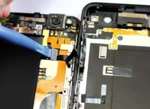
Perhaps the most visible (or invisible, depending on how you look at it) application is in our personal electronics. That smartphone in your pocket contains multiple flexible circuits, allowing manufacturers to cram more functionality into increasingly thin devices. The connecting circuits between your phone’s main board and its camera, display, and battery? All flexible PCBs. Those impossibly thin laptops? Flex PCBs routing signals through the hinges. Smartwatches and fitness trackers? Absolutely packed with flexible circuits.
And let’s not forget the emerging applications that sound like science fiction but are very much science fact. Low-altitude airspace innovations like drones, air taxis, and eVTOL (Electric Vertical Takeoff and Landing) vehicles rely heavily on flexible PCB technology to reduce weight while maintaining reliability. Every gram matters when you’re trying to keep something in the air, and flexible circuits deliver functionality without the bulk.
Quality Control: Boot Camp for Bendy Circuits
Now, you might think that after manufacturing, these flexible circuits just get tossed into a box and shipped off to become the brains of your next gadget. Oh, how wrong you’d be! The testing and quality control for flexible PCBs is more intense than a reality show competition.
First comes electrical testing, where each circuit is checked for continuity and isolation. Think of it as making sure all the roads connect to the right destinations and there are no unexpected shortcuts. This happens through flying probe tests or specialized fixtures that make contact with every testable point on the circuit.
But electrical testing is just the beginning. Flexibility testing is where things get interesting. Imagine a machine designed specifically to bend, fold, and twist your circuit thousands of times while monitoring for any failures. It’s basically a torture chamber for electronics, ensuring that when your smartphone flips open and closed or your car’s side mirror adjusts thousands of times, the circuits inside won’t give up the ghost.
Environmental testing takes this to another level. Circuits are subjected to temperature extremes that would make a polar bear and desert camel equally uncomfortable, humidity levels ranging from bone-dry to tropical rainforest, and vibration tests that simulate everything from a bumpy car ride to a rocket launch.
“We had one client who needed circuits for a mining application,” recalls a Flex Plus testing engineer. “These circuits needed to work reliably inside smart helmets in environments with extreme heat, dust, and constant vibration. The testing regimen was brutal – but that’s exactly what ensures these circuits won’t fail when someone’s safety depends on them.”
For specialized applications like medical devices or automotive components, the testing becomes even more rigorous. ISO 13485 certification for medical applications and IATF 16949 for automotive ensure that flexible PCB manufacturers like Flex Plus meet internationally recognized standards for quality and reliability.
The Flexible Future: Tomorrow’s Bendy Innovations
As we peer into the crystal ball of technology, flexible PCBs are positioned to enable some of the most exciting innovations on the horizon.
Augmented reality (AR) wearables and AI glasses represent a massive opportunity for flexible circuits. These devices need to be lightweight, comfortable, and pack significant computing power into frames barely larger than regular eyeglasses. Without the space-saving and conformability of flexible PCBs, these devices would remain bulky prototypes instead of the sleek consumer products currently emerging.
The beauty tech industry is another unexpected frontier. From smart mirrors that analyze your skin to high-tech facial massagers and LED therapy masks, flexible PCBs are enabling beauty gadgets that would have seemed like science fiction just a few years ago.
Perhaps most exciting is the development of transparent flexible PCBs. Imagine electronics that you can literally see through, enabling circuits that can be integrated into windows, displays, or even contact lenses without blocking vision. Flex Plus has been pioneering this technology, creating circuits that combine flexibility with transparency for next-generation applications.
Stretchable circuits represent another leap forward. Traditional flexible PCBs can bend but not stretch – limiting their applications in certain wearables or medical devices that need to conform to irregular shapes or expand and contract. New TPU (Thermoplastic Polyurethane) circuits can actually stretch while maintaining electrical functionality, opening up entirely new design possibilities.
“The most exciting innovations are happening at the intersection of flexible PCB manufacturing and other technologies,” explains a Flex Plus R&D engineer. “When you combine flexible circuits with advanced COB (Chip-on-Board) integration, you can create electronic assemblies that are thinner, more reliable, and more capable than anything possible with traditional manufacturing.”
As our devices continue to get smaller, more complex, and more integrated into our daily lives, flexible PCB manufacturing will continue to evolve, bend, and flex to meet these challenges. From the smartphone in your pocket to the electric vehicle in your garage and the medical device monitoring your health, these bendy wonders are working behind the scenes, enabling the technology that shapes our world.
So next time you marvel at how thin your laptop is or how your fitness tracker conforms perfectly to your wrist, spare a thought for the flexible PCBs inside – the unsung heroes of the electronics world, bending the rules of what’s possible one circuit at a time.