
When you hold a smartphone, medical monitor, or electric vehicle control module, you’re holding thousands of precisely placed components working together as one system. But how does a bare circuit board transform into a functioning device? The answer lies in PCB assembly—a critical manufacturing process that determines whether your product succeeds or fails in the market.
PCB assembly, or PCBA, is the process of mounting electronic components onto a printed circuit board to create a complete, functional circuit. While PCB fabrication creates the conductive pathways, assembly brings the board to life by adding the components that process signals, store data, and power your device.
This distinction matters enormously. A bare PCB is just copper traces on substrate material. A fully populated assembly is a working electronic system ready for integration into your final product. For engineers in automotive, medical, industrial, and consumer electronics sectors, understanding this process isn’t optional—it’s essential for designing products that can actually be manufactured at scale with consistent quality.
The stakes are particularly high in sectors requiring certified solutions. An automotive ECU assembly must meet IATF 16949 standards. Medical device PCBAs need ISO 13485 compliance. Industrial control systems demand long-term reliability under harsh conditions. Consumer electronics require high-volume production at competitive costs. Each application demands different approaches, but all share the same foundation: a thorough understanding of the assembly process from the earliest design stages.
The Building Blocks: Components That Make PCBAs Work
Every functional PCBA relies on three fundamental component categories, each serving distinct roles in your circuit’s performance.
Passive components form the foundation of most assemblies. Resistors control current flow, capacitors store and release energy, and inductors manage magnetic fields. These components seem simple, but their placement and selection directly impact signal integrity and power distribution. A 0201-size resistor measures just 0.6mm × 0.3mm—smaller than a grain of sand—yet must be placed with micron-level precision to function correctly in high-density designs.
Active components perform the processing work. Integrated circuits (ICs) execute logic operations, transistors amplify signals, and microcontrollers serve as the brain of your system. These components often generate significant heat and require careful thermal management. In flexible PCB applications, this challenge intensifies—FlexPlus has developed breakthrough flexible heat dissipation flow channels specifically to address thermal management in bendable circuits where traditional heatsinks won’t work.
Interconnects tie everything together. Connectors enable board-to-board communication, via structures create paths between layers, and solder joints provide both electrical and mechanical connections. In rigid-flex designs, these interconnections become even more critical. FlexPlus’s rigid-flex solutions eliminate up to 87% of traditional interconnection points by seamlessly integrating flexible and rigid sections, dramatically improving reliability in applications where connector failures would be catastrophic—like aerospace systems or medical implants.
The interaction between these components determines your product’s functionality. A medical wearable monitoring heart rate needs ultra-thin construction (FlexPlus achieves down to 25 microns with gold plating on double-sided flex PCB), flexible substrate for patient comfort (TPU circuits with medical-grade materials), and precise component placement (COB technology with ±5° wafer offset angle tolerance). Each component category plays its part in creating a device that’s both functional and manufacturable.
Two Fundamental Assembly Methods: SMT and THT
Modern PCBA relies primarily on two assembly techniques, each with distinct advantages and applications.
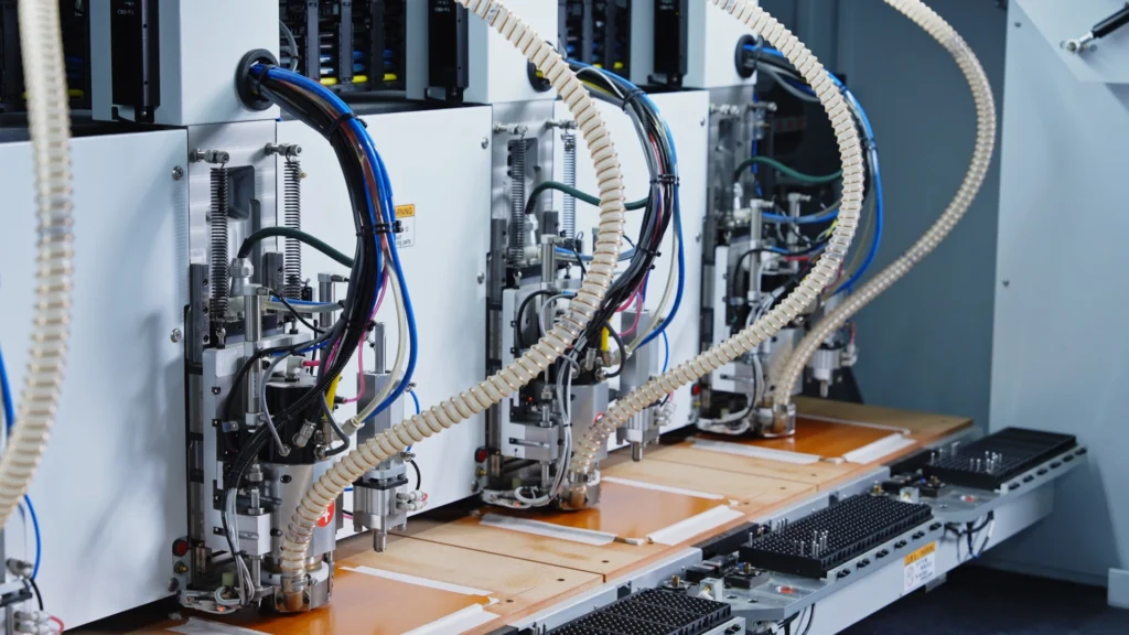
Surface Mount Technology (SMT) has become the dominant approach for high-density, high-volume production. Components mount directly onto the board surface without drilling holes, enabling dramatic miniaturization. The process begins with solder paste printing—a stencil deposits precise amounts of solder paste onto PCB pads. Automated pick-and-place machines then position components with remarkable speed and accuracy, placing thousands of parts per hour. Finally, reflow soldering melts the solder paste in a controlled temperature profile, creating permanent connections.
SMT’s advantages are compelling for modern electronics. Component density increases dramatically—you can place parts on both sides of the board with minimal spacing. Production speed accelerates since automated equipment handles most operations. Board weight decreases because components lack long leads. These benefits explain why smartphones, wearables, and most consumer electronics rely exclusively on SMT.
However, SMT presents challenges in flexible PCB assembly. The reflow process subjects boards to temperatures approaching 260°C, which can stress flexible substrates. FlexPlus addresses this through careful material selection and process control, using polyimide substrates that maintain dimensional stability during reflow while retaining flexibility after assembly. For ultra-thin applications down to 25 microns, this thermal management becomes even more critical—a challenge our 20+ years of specialized experience helps customers navigate successfully.
Through-Hole Technology (THT) involves inserting component leads through drilled holes and soldering them on the opposite side. While older than SMT, THT remains essential for specific applications. Components requiring high mechanical strength—heavy connectors, transformers, or electromechanical switches—often use through-hole mounting. Testing points and components requiring manual replacement also benefit from THT’s accessibility.
The THT process differs significantly from SMT. After components are inserted (either manually or by automated insertion equipment), wave soldering passes the board over a molten solder wave that fills holes and creates joints simultaneously. Selective soldering offers more precision for mixed-technology boards, applying solder only where needed without affecting previously assembled SMT components.
Many production PCBAs use both technologies. A typical automotive control module might use SMT for dense logic circuits and THT for robust power connectors. This mixed-technology approach requires careful process sequencing—typically SMT first, then THT—to avoid damaging previously assembled components.
The Complete PCBA Process Flow: From Bare Board to Finished Assembly
Understanding the full production sequence helps engineers design boards that move smoothly through manufacturing.
The process begins with PCB fabrication—creating the bare board with its copper traces, via structures, and surface finishes. For flexible circuits, this stage includes critical decisions about materials, stackup configuration, and reinforcements. FlexPlus‘s capability extends from single-sided FPC through 8-layer flexible and 12-layer rigid-flex designs, with specialized options like sculptured FPC and TPU circuits for applications requiring extreme flexibility or biocompatibility.
Solder paste application follows for SMT assembly. Screen printing deposits paste with precision—typically ±25 microns for fine-pitch components. The stencil thickness, aperture design, and paste composition all affect joint quality. Solder paste inspection (SPI) systems verify deposits before component placement, catching print defects before they become assembly failures.
Component placement positions parts according to your design file. Modern pick-and-place systems achieve placement accuracy within ±0.02mm, essential for fine-pitch ICs and 0201-size passives. For flexible circuits, this stage requires specialized fixtures to maintain board flatness during placement. FlexPlus‘s innovative magnetic fixture technology addresses the uneven substrate challenge inherent in flexible materials, ensuring consistent placement accuracy even on ultra-thin designs.
Reflow soldering creates permanent solder joints through controlled heating. The temperature profile—preheat, thermal soak, reflow, and cooling—must match your components’ specifications and board materials. Flexible substrates require particular attention since excessive heat or rapid temperature changes can cause warping or delamination.
Through-hole assembly follows if your design includes THT components. Wave soldering or selective soldering creates joints while protecting previously assembled SMT parts with appropriate masking or fixtures.
Quality inspection occurs at multiple points throughout the process. Automated Optical Inspection (AOI) uses high-resolution cameras to detect component placement errors, polarity mistakes, or solder defects. X-ray inspection (AXI) reveals hidden issues in BGA packages, via fills, or complex stackups. In-Circuit Testing (ICT) verifies electrical connections and component values. Functional testing confirms the assembled board performs as designed under real operating conditions.
For advanced applications, FlexPlus offers flexible substrate COB technology—directly mounting bare chips onto flexible circuits. This breakthrough approach achieves industry-leading precision with wafer offset angle tolerance within ±5° and COB encapsulation thickness tolerance within 50-100μm (±25-50μm). This micron-level precision enables ultra-thin designs while maintaining reliability, critical for applications like AR glasses or medical wearables where every tenth of a millimeter matters.
Finally, packaging and protection prepares assemblies for integration. Conformal coating protects against moisture and contaminants. Protective coverlays shield flexible circuits during handling. Proper packaging prevents damage during shipping to your facility.
Designing for Manufacturing Success: DFM and Compliance Considerations
The best time to optimize assembly is during design—long before production begins. Design for Manufacturing (DFM) principles help engineers create boards that assemble reliably at high volumes.
Component spacing directly impacts yield. IPC-A-610 standards specify minimum clearances between components, but experienced manufacturers recommend exceeding minimums. Tight spacing between tall and short components creates shadowing during reflow, leading to insufficient heating. On flexible circuits, adequate spacing around bend areas prevents stress concentrations that cause failures.
Pad design must support both assembly and reliability. Pad size affects solder joint strength—too small creates weak joints, too large causes bridging. For fine-pitch components, non-solder mask defined (NSMD) pads typically outperform solder mask defined (SMD) pads. FlexPlus‘s minimum line width/space capability of 0.05mm/0.05mm (2mil/2mil) enables high-density designs, but requires corresponding attention to pad geometry.
Orientation and polarity marking prevents assembly errors. Clear component designators, polarity indicators, and fiducial marks enable both automated systems and human operators to place parts correctly. This becomes especially important in flexible circuits where visual inspection may be more challenging due to substrate translucency or flexibility.
Testability considerations should be built in from the start. Test points at critical nodes enable ICT verification. Adequate clearance around test points ensures probe access. For complex assemblies, built-in self-test (BIST) capabilities reduce reliance on external test equipment.
Regulatory compliance varies by industry but always requires planning. Automotive applications demand IATF 16949 certification—not just of the assembler but throughout the supply chain. Medical devices require ISO 13485 compliance with complete traceability. Industrial controls may need specific environmental certifications. FlexPlus holds all major international certifications (ISO 9001, ISO 13485, IATF 16949, ISO 14001), but engineers must still design products that can demonstrate compliance through testing and documentation.
The bill of materials (BOM) deserves particular attention. Specify components with clear manufacturer part numbers, avoid obsolete or hard-to-source parts, and consider second-sourcing for critical components. A poorly managed BOM can delay production by weeks or months, regardless of how well the board is designed.
Common Defects and How to Prevent Them
Even with careful planning, assembly defects occur. Understanding common failure modes helps engineers design more robust products.
Solder joint defects account for the majority of assembly problems. Insufficient solder creates weak joints prone to failure under thermal cycling or vibration. Excessive solder causes bridging between adjacent pads, creating shorts. Voids within joints reduce mechanical strength and thermal conductivity. Cold solder joints result from inadequate reflow temperature or contaminated surfaces. Prevention requires proper pad design, controlled reflow profiles, and clean board surfaces.
Component placement errors include wrong orientation (particularly problematic with polarized components like diodes or electrolytic capacitors), shifted position, or missing components. AOI catches most placement errors, but clear silkscreen markings and component polarity indicators prevent errors in the first place.
Warping and delamination particularly affect flexible circuits. Thermal stress during reflow can cause substrate warping if temperature profiles aren’t optimized for flexible materials. Delamination between layers indicates adhesive failure or excessive moisture absorption. FlexPlus‘s process control ensures polyimide-based flexible circuits maintain dimensional stability throughout assembly, even in designs as thin as 25 microns.
Tombstoning occurs when one end of a small chip component lifts during reflow, creating an open circuit. Uneven heating, asymmetric pad designs, or incorrect paste volume all contribute. Balanced pad layouts and controlled heating rates prevent this defect.
Via failures in multilayer boards create intermittent or complete circuit failures. Inadequate via fill, barrel cracking during thermal cycling, or contamination during fabrication all cause problems. X-ray inspection reveals most via defects before they reach the field.
For flexible and rigid-flex assemblies, additional failure modes emerge. Stress fractures occur at rigid-flex transition zones if bend radii are too tight or if component placement doesn’t account for flex areas. Adhesive failures between layers cause delamination under thermal cycling. Conductor cracking results from excessive bending or inadequate copper thickness. FlexPlus‘s 20+ years of flexible circuit expertise helps customers avoid these pitfalls through comprehensive DFM review before production begins.
Prototyping vs. Volume Production: Different Approaches for Different Stages
The journey from concept to mass production involves distinct phases, each with different priorities.
Prototyping emphasizes speed and flexibility. Engineers need boards quickly to validate designs, test functionality, and identify issues. Small quantities (often 5-50 boards) allow rapid iteration without enormous investment. FlexPlus offers standard turnaround within one week and emergency requests in three days, enabling fast design cycles. At this stage, DFM issues can be corrected, component selections refined, and assembly processes optimized before committing to volume production.
Prototype assembly often uses less automation—more hand placement, more visual inspection, more functional testing. This approach makes sense when quantities are small and design changes are likely. However, prototypes should still follow production-quality processes. A prototype that works perfectly but can’t be manufactured reliably at volume creates costly problems later.
Volume production shifts priorities to cost, consistency, and speed. Automated assembly becomes essential—pick-and-place machines place thousands of components per hour with consistent accuracy. Process control tightens—reflow profiles are fine-tuned, inspection criteria are quantified, and statistical process control monitors trends. Supplier relationships matter enormously—securing reliable component sources at competitive prices directly impacts profitability.
The transition from prototype to volume production often reveals hidden issues. A hand-placed component that worked fine in prototypes may require different pad geometry for automated placement. A reflow profile perfect for 10 boards might need adjustment for 10,000 boards processed continuously. FlexPlus‘s full in-house capabilities from raw material to final inspection eliminate the communication gaps and quality inconsistencies that emerge when working with brokers or trading companies managing multiple subcontractors.
Supply chain management becomes critical at volume. Lead times for specialized components can extend to months. Price fluctuations affect margins. Component obsolescence requires redesigns. A well-managed BOM with second-source options and early supplier engagement prevents production delays. FlexPlus‘s comprehensive assembly services include component sourcing, reducing vendor count and minimizing the coordination challenges that delay production schedules.
The Future of PCB Assembly: Emerging Trends and Technologies
Assembly technology continues evolving rapidly, driven by demands for smaller, faster, more reliable devices.
High-Density Interconnect (HDI) designs push miniaturization further. Microvias—laser-drilled holes as small as 0.1mm—create connections between layers without consuming precious board real estate. Sequential build-up layers add circuitry in stages rather than all at once. These technologies enable smartphone-level density in flexible circuits, opening new application possibilities.
Advanced packaging techniques like COB (Chip-on-Board) eliminate the package around semiconductor dies, mounting bare silicon directly onto substrates. FlexPlus’s flexible substrate COB technology represents a breakthrough in this field, achieving industry-leading precision with die bonding offset angle tolerance within ±5° and encapsulation thickness tolerance within ±25-50μm. This approach creates ultra-thin assemblies while maintaining the flexibility that rigid boards cannot provide—essential for wearables, medical devices, and beauty tech applications where conforming to curved surfaces matters.
AI-driven automation optimizes assembly processes in real-time. Machine vision systems detect defects invisible to human operators. Predictive maintenance prevents equipment failures before they occur. Process parameter optimization reduces defects while increasing throughput. These technologies require sophisticated manufacturing infrastructure but deliver dramatic quality and efficiency improvements.
Sustainable manufacturing addresses environmental concerns. Lead-free solders eliminate toxic materials. Water-soluble fluxes replace harsher solvents. Recycling programs recover precious metals from scrap. FlexPlus‘s ISO 14001 certification demonstrates commitment to environmental responsibility while maintaining the quality standards critical sectors demand.
The convergence of these trends creates exciting possibilities. Imagine medical implants with flexible circuits conforming to body contours, featuring direct chip attachment for minimal thickness, manufactured with AI-optimized processes ensuring consistent quality. Or autonomous vehicle sensors with HDI flexible circuits providing both high component density and mechanical flexibility, assembled with zero-defect quality through advanced inspection systems.
Moving Forward: Best Practices for Engineering Success
PCB assembly transforms your design from concept to functioning product. The engineers who understand this process—really understand it, from solder paste rheology to supply chain logistics—create products that move smoothly from prototype to mass production.
Start with manufacturability from day one. Don’t wait until prototypes are built to think about assembly. Engage your manufacturing partner early, review DFM guidelines, and incorporate feedback into initial designs. FlexPlus offers comprehensive design support precisely because catching issues early saves months of iteration.
Choose materials strategically. In flexible circuits, substrate selection affects everything from assembly temperatures to long-term reliability. Polyimide offers excellent thermal stability for reflow soldering. TPU provides biocompatibility for medical applications. FR-4 backed areas in rigid-flex designs provide mounting support where needed. Material consultation from experienced manufacturers prevents costly mistakes.
Design with inspection in mind. AOI systems need clear visual access to component markings. X-ray inspection requires understanding how different materials appear in radiographs. ICT needs accessible test points. Building inspectability into designs improves yield and reduces troubleshooting time.
Validate early and often. Prototype iterations catch problems that simulation misses. Real-world assembly reveals issues that design files don’t show. Functional testing under actual operating conditions finds problems before customers do.
Partner with manufacturers who control their entire process. Direct communication with production engineers eliminates the miscommunication and quality inconsistencies that plague broker-managed production. FlexPlus‘s end-to-end control from raw material to final inspection, combined with 20+ years of flexible circuit specialization, provides the expertise and reliability that high-stakes applications demand.
PCB assembly isn’t just a manufacturing step—it’s where engineering vision becomes reality. Understanding this process empowers you to design products that not only function beautifully but can actually be manufactured at the quality, volume, and price your market demands. Whether you’re developing automotive electronics requiring IATF 16949 certification, medical devices needing ISO 13485 compliance, or consumer products demanding competitive costs, the assembly process fundamentals remain the same: careful planning, appropriate technology selection, and partnership with manufacturers who genuinely understand the challenges you face.
The next time you design a circuit, think beyond schematic and layout. Think about solder paste printing on those tiny pads, automated placement of hundreds of components, reflow temperatures affecting your flexible substrate, and inspection systems verifying every joint. Think about the complete journey from bare board to functioning assembly. That holistic perspective transforms good engineers into great ones—and good products into market successes.