
The electronics industry stands at a crossroads. As consumer expectations drive demand for sleeker, lighter, and more capable devices, traditional circuit board designs have reached their physical limits. While conventional PCB assembly processes excel at rigid board production, they struggle with the extreme miniaturization demands of next-generation wearables. Rigid PCBs with surface-mounted components can only shrink so far before mechanical constraints and assembly complexities halt progress. Enter Flexible Chip-on-Board (COB) Integration—a transformative approach that’s rewriting the rules of miniaturization.
This technology represents more than incremental improvement. By mounting bare silicon dies directly onto flexible substrates like polyimide or ultra-thin PET, Flexible COB Integration eliminates the packaging bulk that has historically constrained device design. The result? Circuit assemblies measuring just 100-200 microns in total thickness, bending radii under 1mm, and form factors that conform seamlessly to curved surfaces. For wearable health monitors that must disappear against skin, AR glasses requiring featherweight optics, or next-generation IoT nodes embedded in industrial equipment, this shift from rigid to flexible represents the difference between conceptual possibility and commercial reality.
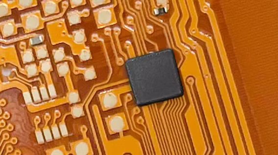
The implications extend beyond thickness alone. Traditional Surface Mount Device (SMD) assembly requires pre-packaged components—each chip encased in plastic or ceramic housing that adds volume, weight, and thermal barriers. Flexible COB strips away these layers, creating unified circuitry where multiple dies share common interconnects with minimal resistance gaps. This architectural simplification doesn’t just save space; it fundamentally changes how engineers approach system integration, opening pathways to previously impossible product categories.
Materials and Processes: Engineering the Invisible
The foundation of Flexible COB Integration rests on breakthrough advancements in substrate engineering and precision assembly. At its core, this technology depends on ultra-thin flexible base materials that maintain dimensional stability under thermal stress while accommodating repeated flexing cycles. Polyimide films, particularly those in the 25-50 micron thickness range, have emerged as the gold standard. These materials exhibit exceptional thermal resistance (continuous operation above 200°C), low moisture absorption, and mechanical properties that allow bend radii approaching 0.5mm without cracking.
The manufacturing process begins with wafer thinning—a critical step that reduces silicon die thickness from standard 525 microns to 50-100 microns or less. This isn’t merely mechanical grinding; advanced back-grinding and chemical-mechanical polishing techniques create uniform thickness across entire wafers while maintaining die strength. The thinned wafers are then singulated into individual chips, ready for direct attachment to flexible substrates.
Direct chip attachment employs specialized anisotropic conductive adhesives (ACAs) that conduct electricity vertically through conductive particles while remaining insulating laterally. During assembly, precise placement equipment positions dies with tolerances under ±10 microns—a requirement driven by the fine pitch interconnects common in modern integrated circuits. Here, FlexPlus’s industry-leading die bonding precision becomes crucial. Our magnetic fixture technology addresses the fundamental challenge of flexible substrates: maintaining planarity during assembly. Unlike rigid boards that provide inherent stability, flexible materials tend to warp under localized heating. Our proprietary magnetic fixturing system applies uniform clamping force across the substrate, controlling wafer offset angles within ±5° and ensuring consistent bonding quality even on materials as thin as 25 microns.
The thermal bonding cycle must be carefully controlled. ACAs typically cure between 150-180°C for 10-30 seconds under controlled pressure. Too much heat damages the flexible substrate or warps the assembly; too little results in incomplete particle deformation and poor electrical contact. This is where two decades of manufacturing experience translate directly into yield improvements. Our process engineers have mapped thermal profiles for hundreds of substrate-adhesive combinations, enabling first-pass success rates exceeding 98% even with complex multi-die layouts.
After die attachment, encapsulation protects the bare silicon and wire bonds from environmental damage. Here again, thickness control becomes paramount. Standard glob-top epoxies produce domes several hundred microns high—unacceptable for ultra-thin applications. FlexPlus has developed ultra-fine dam encapsulation processes where protective barriers are formed with thickness tolerances of just ±5 microns, and total COB package height is controlled within 50-100 microns (±25-50 microns). This micron-level precision packaging allows completed assemblies to maintain flexibility while providing robust chip protection, creating what industry insiders call “compliant system integration.” For detailed insights into advanced COB LED lighting applications and purchase considerations, manufacturers can reference comprehensive technical guides, creating what industry insiders call “compliant system integration.”
Packaging and Interconnect: Connecting the Dots
The interconnection strategy in Flexible COB fundamentally differs from traditional PCB assembly. Two primary approaches dominate: flip-chip on flex and face-up wire bonding, each suited to specific application requirements.
Flip-chip on flex represents the highest density interconnect method. The silicon die is inverted and bonded face-down onto the flexible substrate, with solder bumps or conductive adhesive making direct contact between chip I/O pads and substrate traces. This configuration minimizes interconnect length—critical for high-speed signals where parasitic inductance and capacitance degrade performance. The compact footprint allows designers to route hundreds of connections within millimeter-scale areas, enabling multi-chip modules that would be impossible with wire bonding.
However, flip-chip demands extraordinary substrate flatness and thermal expansion matching. During reflow or ACF bonding, temperature excursions approaching 250°C cause both silicon and substrate to expand. Coefficient of thermal expansion (CTE) mismatches create shear stresses at the bond interface that can crack solder joints or delaminate adhesive. Polyimide’s CTE (typically 12-16 ppm/°C) reasonably matches silicon (2.6 ppm/°C), but careful substrate design—including copper trace geometry that controls expansion—remains essential. Our design-for-manufacturing support includes finite element analysis of thermal stress patterns, recommending trace layouts that distribute forces evenly across the bond array.
Face-up wire bonding offers greater flexibility in die attachment but requires more vertical space. Similar principles apply to flexible PCB assembly, where component placement and bonding techniques must account for substrate movement. The chip bonds face-up to the substrate, with gold or aluminum wires—each 15-25 microns in diameter—connecting chip bond pads to substrate traces. This traditional technique adapts well to flexible substrates, particularly when magnetic fixturing stabilizes the material during ultrasonic bonding. Wire loops extend 100-200 microns above the die surface, setting minimum encapsulation thickness. For many wearable applications where 200-300 micron total thickness remains acceptable, wire bonding provides proven reliability at lower tooling costs than flip-chip.
Thermal management in Flexible COB assemblies presents unique challenges. Unlike rigid boards with thick copper layers acting as heat spreaders, thin flexible substrates offer minimal thermal conduction paths. High-power chips can create localized hot spots, accelerating material degradation. FlexPlus addresses this through innovative thermal pathway integration. Our proprietary flexible heat dissipation flow channels incorporate copper-filled via arrays and embedded thermal planes within multilayer flexible constructions. These channels route heat away from die locations toward device peripheries where convection or conduction to housing can dissipate it. In applications like high-power LED modules and automotive sensor nodes operating in 85°C+ ambient temperatures, these thermal solutions reduce junction temperatures by 15-30°C—directly translating to improved reliability and extended operational lifetimes.
Mechanical reliability strategies acknowledge that flexible assemblies will bend, twist, and flex throughout their service lives. Standard rigid PCB reliability testing—temperature cycling and vibration—must be augmented with dynamic flexure protocols. Industry standards like IPC-6013 specify bend testing at defined radii, but real-world applications often subject assemblies to complex multi-axis motion. Our reliability validation includes custom flex testing that simulates actual device usage patterns, from the wrist movements of fitness trackers to the folding cycles of foldable displays. Accelerated life testing typically involves 100,000+ flex cycles at minimum bend radius, ensuring designs withstand years of field use.
Application Hotspots: Where Flexibility Meets Function
Flexible COB Integration has found its most compelling applications in three fast-growing sectors: wearables, AR/VR devices, and next-generation IoT nodes. Each benefits distinctly from the technology’s unique advantages.
Wearable health monitors represent perhaps the most demanding application. Recent advances in miniaturized wearable biosensors for continuous health monitoring demonstrate the critical importance of biocompatible flexible substrates. Devices like continuous glucose monitors, ECG patches, and sleep trackers must conform intimately to skin while remaining virtually imperceptible. A 300-micron thick assembly feels bulky against the body; 150 microns or less achieves skin-like compliance. FlexPlus has developed biocompatible Flexible COB solutions using medical-grade polyimide substrates and encapsulants approved for skin contact. These assemblies integrate analog front-end chips for biosignal acquisition, microcontrollers for processing, and Bluetooth system-on-chips for wireless connectivity—all on circuits measuring just 20mm × 30mm with total thickness under 200 microns. The weight savings are dramatic: comparable SMD-based designs weigh 3-5 grams, while our COB assemblies achieve the same functionality at under 1 gram.
The competitive advantage over traditional SMD extends beyond size. Pre-packaged SMD components each add thermal resistance between the silicon die and substrate—the plastic or ceramic package acts as insulation. In COB assemblies, dies bond directly to the substrate with minimal thermal interface material, reducing junction-to-ambient thermal resistance by 40-60%. For wearables powered by tiny batteries, this efficiency translates directly to longer runtime or smaller battery requirements. Moreover, with fewer discrete components to source and place, assembly process steps reduce from 30-40 operations to 10-15, cutting manufacturing time and cost while improving yield.
AR glasses and VR headsets demand Flexible COB for different reasons: ultra-light weight and conformability to complex optical geometries. Consider AR display drivers mounted on curved waveguide surfaces. Traditional rigid PCBs require bulky mechanical mounting schemes with compliance interfaces. Flexible COB assemblies laminate directly onto curved optics, distributing driver electronics across the optical path in ways that balance weight and minimize optical interference. Several leading AR platforms now incorporate our flexible COB technology in their display modules, achieving display driver densities exceeding 300 chips per cubic centimeter while maintaining assembly weights under 5 grams per module.
Next-generation IoT sensor nodes increasingly require electronics embedded in mechanically challenging locations. Our rigid-flex PCB construction expertise enables seamless integration of rigid and flexible sections for these demanding applications—wrapped around pipes for industrial monitoring, integrated into rotating machinery, or embedded in inflatable structures. These applications demand circuits that survive continuous flexing and extreme environmental exposure while providing multi-sensor integration in minimal space. Our rigid-flex COB solutions combine rigid sections for mounting components like batteries and connectors with flexible COB regions containing sensor interface chips and processing logic. This architectural approach eliminates the mechanical stress concentrations that plague cable-connected rigid assemblies, reducing field failure rates by an order of magnitude in demanding industrial environments.
Manufacturing Challenges and Solutions
Despite compelling advantages, Flexible COB Integration presents manufacturing challenges that have historically limited widespread adoption. Quality and yield control demand systematic approaches addressing three critical areas: substrate handling, die attach precision, and encapsulation uniformity.
Flexible substrate handling begins with material selection and preparation. Understanding flexible circuit board design guidelines is essential before entering production, as material properties directly impact handling protocols. Unlike rigid FR-4 boards that maintain dimensional stability through processing, flexible polyimide can distort under temperature, humidity, or mechanical stress. Our manufacturing process employs environmentally controlled areas maintaining 23°C ±2°C and 50% ±5% relative humidity. Substrates are vacuum-laminated to temporary rigid carriers before entering assembly, providing the mechanical stability needed for precision placement while preserving flexibility in the final product. After assembly completion, controlled peel-off releases the finished COB assembly without inducing stress that could crack die attach bonds or damage interconnects.
Die attach precision determines electrical performance and long-term reliability. Misalignment of just 20 microns on fine-pitch devices can cause open circuits or marginal connections that fail under thermal cycling. FlexPlus employs vision-guided placement systems with pattern recognition algorithms that automatically correct for substrate distortion, thermal expansion, and placement drift. Our equipment achieves placement accuracy of ±8 microns at 3σ—industry-leading precision that enables reliable flip-chip attachment on flexible substrates even with pitch below 100 microns. This precision comes from our investment in advanced motion control systems and proprietary magnetic fixturing that maintains substrate flatness within 10 microns across 300mm × 400mm panels.
Encapsulation uniformity affects both protection and flexibility. Thick or uneven encapsulation creates stiff regions that concentrate mechanical stress during flexing, eventually causing fatigue cracks. Our automated dispensing systems employ closed-loop vision feedback that monitors dam height and encapsulant coverage in real-time, adjusting dispense parameters mid-cycle to maintain the ±5 micron thickness tolerance that preserves flexibility. This level of control requires specialized low-viscosity encapsulants formulated specifically for ultra-thin applications—materials we’ve developed through partnerships with leading chemical suppliers.
Process standards and ecosystem development remain critical needs. Industry organizations like AVIXA provide guidance on Chip on Board LED applications in professional AV environments, while broader electronics standards continue evolving to address flexible COB integration. Unlike rigid PCB assembly with mature IPC standards and widespread industry knowledge, Flexible COB practices vary significantly between manufacturers. FlexPlus actively participates in standards development through industry organizations, contributing our 20+ years of experience toward codifying best practices for flexible COB manufacturing. Our ISO 9001, ISO 13485, IATF 16949, and ISO 14001 certifications demonstrate commitment to systematic quality management, while our internal process documentation provides customers with transparent insight into our manufacturing methodologies.
Future Outlook: The Long-Term Impact
As we look ahead, Flexible COB Integration stands poised to enable product categories barely imaginable with traditional technology. The convergence of ultra-thin substrates, precision die assembly, and advanced encapsulation creates a platform for truly imperceptible electronics—devices that integrate seamlessly into clothing, furniture, vehicles, and architectural elements.
Medical applications will expand dramatically as biocompatible materials and processes mature. Imagine implantable diagnostic monitors assembled on TPU substrates that flex and stretch with living tissue, or wound healing accelerators with integrated sensors monitoring recovery in real-time. FlexPlus’s pioneering work in TPU circuits positions us to support these next-generation bioelectronics applications, combining our flexible COB expertise with medical-grade materials that meet ISO 13485 requirements.
The automotive sector will increasingly adopt Flexible COB for safety-critical sensors embedded in complex interior geometries—steering wheels, seats, and dashboard surfaces requiring high-reliability electronics that conform to ergonomic shapes. Our IATF 16949 certification and proven thermal management technologies address the automotive industry’s stringent quality and environmental requirements, enabling partnerships with leading EV manufacturers and Tier 1 suppliers.
This technological evolution aligns perfectly with FlexPlus’s philosophy of certified excellence and engineering partnership. We don’t simply manufacture flexible circuits; we collaborate with customers from concept through mass production, applying our comprehensive capabilities—from advanced R&D to full assembly services—toward solving complex integration challenges. Our investment in breakthrough technologies like magnetic fixture systems and micron-level encapsulation reflects commitment to innovation that drives the industry forward.
For companies developing next-generation wearables, AR devices, or advanced IoT solutions, Flexible COB Integration represents more than a manufacturing technique—it’s an enabling technology that transforms product vision into market reality. With 20+ years of specialized experience, complete in-house manufacturing control, and direct engineering support, FlexPlus stands ready to partner in bringing these innovations to life, one ultra-thin assembly at a time.