
The smartphone in your pocket bends every time you sit down. The medical device monitoring a patient’s vital signs flexes with every movement. The drone soaring through the sky relies on circuits that can withstand constant vibration and temperature changes. What makes all of this possible? Flexible PCB architecture.
Flexible printed circuit boards have revolutionized how we design electronic products. Unlike traditional rigid boards that crack under stress, flexible PCBs can bend, fold, and even twist while maintaining electrical performance. This flexibility has opened doors to innovations across industries—from electric vehicles with sleek head-up displays to wearable AR glasses that fit comfortably on your face. But here’s the challenge: designing a flexible PCB that actually works in the real world requires more than just choosing a bendable material. It demands a deep understanding of design principles that balance performance, reliability, and manufacturability.
Understanding Industry Standards: Your Blueprint for Success
Before you draw a single trace on your flexible PCB design, you need to understand the rules of the game. The IPC-2223 standard isn’t just a suggestion—it’s your roadmap to creating flexible circuits that won’t fail in the field.
Think of IPC-2223 as the constitution for flexible PCB design. This standard, developed by the Institute for Printed Circuits, provides detailed guidelines covering everything from material selection to copper feature placement. When a medical device manufacturer creates an ISO 13485-certified biomedical-compatible device, they’re not guessing about bend radiuses or layer stackups—they’re following IPC-2223 to the letter.
Why does this matter? Consider this real-world scenario: An automotive electronics supplier designed a flexible circuit for an electric vehicle’s camera system without properly consulting IPC-2223. The design looked perfect on paper, but after just six months of testing, the copper traces began cracking at bend points. The company had to recall thousands of units, costing millions of dollars and damaging their reputation. The root cause? They ignored the standard’s guidelines on minimum bend radius calculations based on material thickness and copper weight.
The standard defines critical parameters like how different materials—polyimide and FR-4—should be used in specific sections to prevent warping or delamination. It provides formulas for calculating bend radius by factoring in the material’s modulus of elasticity, copper thickness, and the number of layers in your stackup. Following these standards isn’t bureaucratic red tape; it’s the difference between a product that works and one that fails catastrophically.
At Flex Plus, we’ve seen countless projects succeed because engineers took the time to understand and apply these standards from day one. Our IATF 16949-certified solutions for electric vehicles, for instance, meet or exceed every requirement in IPC-2223, ensuring that circuits in critical automotive applications perform reliably for years.
Essential Design Considerations: Getting the Fundamentals Right
Designing a flexible PCB isn’t like designing a rigid board with flexible material. It requires a fundamentally different approach to three critical areas: bending requirements, material selection, and stack-up configuration.
Bending Requirements: Define Before You Design
Your first question should never be “What material should I use?” It should be “How will this circuit bend in actual use?” A circuit that needs to flex occasionally during installation requires completely different considerations than one flexing thousands of times during operation.
Static flex applications—like circuits folded once during assembly—can tolerate tighter bend radiuses and more layers. Dynamic flex applications—like those in robotic arms or wearable devices—need generous bend radiuses and special attention to copper placement in flex zones. The IPC-2223 standard defines minimum bend radius as a multiplier of flex thickness, but materials like thick copper and heavy adhesive may require you to increase this number significantly.
Material Selection: The Foundation of Reliability
Polyimide remains the gold standard for flexible substrates, offering excellent thermal stability, chemical resistance, and mechanical properties. But not all polyimide films are created equal. The thickness you choose—ranging from 12.5 microns to 125 microns—dramatically affects your circuit’s flexibility, electrical performance, and cost.
For extreme applications requiring biocompatible solutions, materials like TPU (thermoplastic polyurethane) offer stretchability that polyimide cannot match. Flex Plus has pioneered TPU circuits ranging from 10-600mm with copper foil options from 18-70μm, enabling innovations in medical wearables and beauty tech devices that conform to the human body.
The adhesive system matters just as much as the substrate. Adhesive-based constructions offer cost advantages but may suffer in high-temperature environments. Adhesiveless constructions provide superior performance and thinner profiles—Flex Plus can achieve overall thickness as thin as 25 microns with gold plating on double-sided flex PCBs—but come with higher material costs.
Stack-up Configuration: Balancing Performance and Flexibility
Your layer stackup determines everything from signal integrity to bend performance. Single-layer designs offer maximum flexibility but limited routing options. Multilayer designs—Flex Plus manufactures flexible PCBs with 1-8 layers—provide greater circuit density but require careful planning to maintain flexibility.
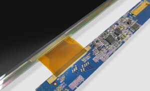
The key is understanding where to place ground planes, how to route signals through flex zones, and when to use rigid-flex combinations. A well-designed rigid-flex board eliminates connectors, reduces assembly complexity, and improves reliability by combining the flexibility of flex circuits with the structural support of rigid sections.
Strategic Copper Feature Placement: Where Reliability Begins
If there’s one design principle that separates successful flexible PCBs from failures, it’s proper copper feature placement. Copper is inherently brittle compared to polyimide substrates, and when you force it to bend repeatedly, it will eventually crack—unless you design intelligently.
The golden rule: never run traces perpendicular to the bend axis in dynamic flex areas. Instead, route traces parallel to the bend line or at 45-degree angles. This simple principle dramatically reduces mechanical stress on the copper during flexing. Think of it like bending a rope versus bending a stick—the rope’s parallel fibers allow it to flex freely, while the stick’s perpendicular grain causes it to break.
Copper weight matters enormously. While ½ oz. copper (17.5 microns) offers good flexibility, thicker copper weights provide better current-carrying capacity and durability. The trade-off requires careful analysis of your specific application. An industrial control system may benefit from 1 oz. copper’s conductivity, while a wearable device prioritizes the flexibility of ½ oz. copper.
Hatched ground planes represent another critical design technique. Instead of solid copper pours in flex areas, use a hatched or crosshatched pattern that allows the substrate to flex more easily while maintaining electrical performance. The spacing and width of these hatches should follow IPC-2223 guidelines based on your flex requirements.
Here’s a real example from the telecommunications sector: An optical transceiver manufacturer initially designed their flexible interconnect with solid copper pours in the flex zone. After 5,000 flex cycles, cracks began appearing in the ground plane. Redesigning with properly hatched copper extended the flex life beyond 100,000 cycles—a 20x improvement that made the difference between product success and failure.
At Flex Plus, our engineering partnership approach includes comprehensive Design for Manufacturing (DFM) analysis that catches these issues before manufacturing begins. We review copper placement, trace routing, and feature sizing to ensure your design will survive real-world conditions.
Cost Optimization: The Balance Between Quality and Economics
Every engineer faces the same challenge: designing a flexible PCB that meets performance requirements while staying within budget. Understanding the cost drivers helps you make intelligent trade-offs without compromising reliability.
Material costs typically represent 30-40% of total flexible PCB expenses. Polyimide substrate, copper foil, coverlay, and adhesives all contribute to this number. Your design decisions directly impact these costs. Choosing thicker polyimide or heavier copper increases material expense. Adding more layers multiplies cost faster than you might expect—a four-layer design doesn’t cost twice as much as a two-layer design; it often costs three or four times more due to processing complexity.
Labor and processing costs account for another 25-35% of your total. This is where manufacturing efficiency comes into play. Designs with tight tolerances, unusual shapes, or complex features require more processing time and careful handling. Our precision capabilities at Flex Plus—including 2/2mil line width/spacing—enable high-density designs, but they come with higher processing costs than standard 4/4mil designs.
Tooling and setup charges represent 10-20% of costs, particularly impactful for prototype and low-volume production. This is where working with a real flexible PCB factory like Flex Plus offers advantages over brokers. We control the entire manufacturing process in our 8,000+ square meter facility, allowing us to optimize tooling costs and offer competitive pricing even for quick-turn prototypes.
The hidden cost that catches many engineers off-guard: assembly complexity. A flexible PCB design that seems cost-effective may require expensive assembly fixtures or specialized handling. Our flex PCBA services address this by providing end-to-end assembly that accounts for the unique challenges of flexible circuits, reducing your vendor count and potential quality issues.
Smart cost optimization isn’t about choosing the cheapest option—it’s about understanding where to invest for maximum return. An electric vehicle manufacturer might spend more on adhesiveless polyimide and thicker copper for circuits in high-temperature, high-reliability applications, while using more economical materials for less critical circuits. This strategic approach to material selection, guided by our technical consultation, helps customers achieve optimal cost-performance balance.
Managing Performance-Manufacturability Trade-offs
The best flexible PCB design on paper means nothing if it can’t be manufactured consistently at scale. This is where understanding the relationship between design ambition and manufacturing reality becomes crucial.
Your CAD library forms the foundation of manufacturability. Using standardized component footprints designed specifically for flexible PCBs ensures that your design can be assembled reliably. Standard rigid PCB footprints often don’t account for the dimensional changes flexible materials undergo during manufacturing and assembly. Temperature variations cause polyimide to expand and contract differently than FR-4, affecting component registration.
Component placement on flexible circuits requires special consideration. Unlike rigid boards where you can place components anywhere on the surface, flexible PCBs have bend zones where components simply cannot go. Placing even a small resistor in a dynamic flex area creates a stress concentration point that will eventually fail. Your component placement strategy must account for these mechanical constraints while still achieving circuit functionality.
Routing strategies for flexible circuits differ fundamentally from rigid board approaches. Smooth, curved traces work better than sharp 90-degree angles. Teardrop pad connections add mechanical strength at the vulnerable junction between traces and pads. Stagger vias in different layers rather than stacking them vertically to avoid creating weak points through the thickness of the stackup.
Consider this example from the aerospace industry: An avionics supplier designed a rigid-flex board with vias stacked directly on top of each other through all six layers, following standard rigid PCB practices. During vibration testing, several of these via stacks fractured, causing intermittent electrical failures. Redesigning with staggered vias—offset by at least 10 mils between layers—eliminated the problem entirely.
The DFM analysis we provide at Flex Plus catches these manufacturability issues early. Our engineers review designs against our 20+ years of manufacturing experience, identifying potential problems before they become expensive mistakes. This proactive approach has helped over 2,500 customers across North America, Europe, Asia, and South America successfully navigate the complex trade-offs between performance ambitions and manufacturing constraints.
Application Excellence Across Industries
The versatility of flexible PCB architecture shines brightest when you see it solving real-world challenges across diverse sectors. Each industry brings unique requirements that push the boundaries of what’s possible with flexible circuits.
In the low-altitude airspace revolution, drones and eVTOL vehicles demand flexible PCBs that withstand extreme vibration, rapid temperature changes, and tight space constraints. Our long flexible PCB capability—up to 3 meters—enables seamless interconnects in drone wing structures and fuselage electronics. The weight savings alone contribute significantly to extended flight times and payload capacity.
The beauty tech industry leverages flexible circuits to create ergonomic devices that conform to facial contours. These applications require both electrical performance and aesthetic considerations—circuits must be thin, flexible, and often transparent. Our breakthrough transparent PCB technology enables beauty gadgets that blend seamlessly with the user experience.
Smart helmets for F1 racing and mining applications integrate sensors, displays, and communication systems in extremely compact spaces. Rigid-flex PCBs eliminate bulky connectors and wiring harnesses, reducing weight and improving reliability in these safety-critical applications. The ability to fold the circuit into three-dimensional shapes enables innovative industrial designs impossible with traditional rigid boards.
Augmented reality wearables and AI-powered glasses represent perhaps the most demanding flexible PCB applications. These devices require ultra-thin flexible circuits—sometimes as thin as 25 microns total thickness—that can bend around temples and conform to frame shapes while delivering high-speed data signals and managing power distribution. Our advanced flexible substrate COB technology takes this further by integrating ultra-thin chips directly onto flexible circuits, achieving levels of miniaturization that traditional packaging cannot match.
Medical devices showcase flexible PCB versatility in life-critical applications. Biocompatible flexible circuits enable implantable sensors, wearable monitors, and surgical instruments that would be impossible with rigid electronics. ISO 13485 certification ensures these devices meet stringent medical industry standards for quality and reliability.
The electric vehicle sector has become a major driver of flexible PCB innovation. From head-up displays to camera systems for autonomous driving, EV manufacturers rely on high-quality flexible circuits that meet IATF 16949 automotive standards. These circuits must survive extreme temperature cycles, moisture exposure, and years of vibration—all while maintaining signal integrity for safety-critical systems.
The Flex Plus Advantage: Innovation Through Partnership
Successfully implementing these seven design principles requires more than theoretical knowledge—it demands practical experience and manufacturing expertise. This is where the Flex Plus philosophy of engineering partnership makes a tangible difference.
Unlike brokers who simply pass your design to unknown manufacturers, Flex Plus offers direct access to factory expertise. Our engineers have spent over 20 years perfecting flexible PCB manufacturing, accumulating deep knowledge of what works and what doesn’t in real-world applications. This experience informs our DFM feedback, technical consultations, and design optimization recommendations.
Our complete manufacturing control—from raw materials to finished assembly—ensures consistency and quality throughout your project lifecycle. We understand how design decisions in the early stages impact manufacturing yield, assembly reliability, and ultimate product performance. This systems-level perspective helps you avoid costly redesigns and production delays.
The certification portfolio we maintain—ISO 9001, ISO 13485, IATF 16949, IPC-6013, ISO 14001—isn’t just paperwork. These certifications represent systematic quality processes that protect your project from quality escapes and compliance issues. When you design to these standards from the beginning, you avoid the expensive retrofitting that plagues projects developed without proper guidance.
Our breakthrough technologies—flexible heat dissipation flow channels, transparent PCBs, ultra-thin designs, and flexible substrate COB integration—expand the realm of what’s possible in your designs. These innovations aren’t developed in isolation; they emerge from collaborating with customers pushing boundaries in industries from aerospace to consumer electronics.
Perhaps most importantly, our rapid prototyping capability—within one week for standard projects, three days for emergency requests—accelerates your development cycle. You can iterate designs quickly, test concepts thoroughly, and reach market faster than competitors working with longer-lead-time suppliers.
Conclusion: Design with Confidence
Flexible PCB architecture represents more than a technological capability—it’s an enabler of innovation across industries reshaping our world. From electric vehicles reducing carbon emissions to medical devices improving patient outcomes, from drones delivering emergency supplies to wearable tech enhancing human capabilities, flexible circuits make the impossible possible.
The seven design principles we’ve explored—understanding standards, optimizing design fundamentals, placing copper strategically, balancing costs, managing trade-offs, and applying industry-specific knowledge—form the foundation of successful flexible PCB projects. Master these principles, and you’ll design circuits that don’t just meet specifications on paper but perform reliably in the real world.
The benefits are compelling: reduced weight that improves product efficiency, enhanced reliability that reduces warranty costs, and design freedom that enables innovative industrial designs. These advantages align perfectly with the needs of industries requiring certified, high-performance flexible PCB solutions.
Your next project doesn’t have to fail. With the right design principles, manufacturing partnership, and commitment to quality, your flexible PCB can become the reliable foundation that makes your product vision a reality. The question isn’t whether flexible PCB architecture can solve your design challenges—it’s whether you’re ready to embrace the principles that make success inevitable.