
When you pick up your smartphone, slide into an electric vehicle, or rely on a medical device to monitor your health, you’re holding the result of countless engineering decisions. Among these, one of the most critical—yet least visible—is the flex-rigid interface design. This junction where flexible circuits meet rigid boards represents a make-or-break moment in electronics manufacturing. Get it wrong, and you’ll face premature failures, signal integrity issues, and costly recalls. Get it right, and you unlock unprecedented design freedom for compact, reliable 3D assemblies.
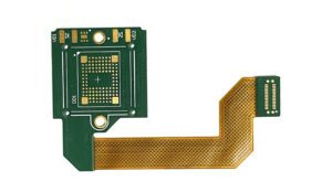
Flex-rigid interface design refers to the engineering discipline of creating seamless transitions between flexible printed circuit boards (FPCBs) and rigid PCB sections within a single assembly. Unlike traditional PCBs that remain entirely flat and rigid, or purely flexible circuits that bend throughout, flex-rigid boards combine both characteristics strategically. This hybrid approach has become essential across industries where space constraints, weight reduction, and mechanical reliability matter most.
In automotive applications, particularly electric vehicles, flex-rigid designs enable complex camera systems, head-up displays, and sensor arrays to fit into tight spaces while withstanding constant vibration. A single flex-rigid board can replace multiple rigid boards connected by cables and connectors, eliminating potential failure points. For aerospace applications, every gram matters—flex-rigid designs reduce weight while improving reliability in extreme conditions. Medical devices benefit from the ability to conform to curved surfaces while maintaining signal integrity for critical measurements. Telecommunications infrastructure relies on these designs to create compact, high-speed modules that fit into increasingly dense server racks.
The beauty of flex-rigid interface design lies in its versatility. A rigid section provides mechanical stability for mounting components and connectors, while flexible sections allow the board to bend, fold, or twist to fit three-dimensional spaces. This eliminates the need for cables, connectors, and multiple separate boards—each of which introduces potential failure points, adds weight, and increases assembly complexity.
The Engineering Challenges That Keep Designers Up at Night
The transition zone between flexible and rigid sections creates a unique set of engineering challenges. This interface represents a meeting point between materials with fundamentally different mechanical properties. Rigid sections, typically made from FR4, remain stiff and dimensionally stable. Flexible sections, usually constructed from polyimide films, can bend repeatedly without damage. Where these two meet, stress concentrates.
Every flex-rigid transition creates a potential weak point. When the board bends during normal operation or assembly, the rigid section acts as an anchor while the flexible section moves. At the junction, copper traces must transition from a supported, stable environment to one that experiences repeated mechanical stress. Without careful design, these traces can crack, delaminate, or develop microscopic fractures that lead to intermittent failures—the worst kind to troubleshoot.
The stackup configuration determines both electrical performance and mechanical reliability. In a typical rigid-flex design, the flexible portion might consist of one or two layers of polyimide with copper traces, while the rigid portion contains four, six, or even eight layers with complex via structures and dense component placement. Managing the transition between these different layer counts requires precise engineering. Air gaps—intentional spaces between layers in the flexible region—help reduce stiffness and improve flexibility, but they also affect impedance control and must be carefully managed for high-speed signals.
Consider a real-world example from the medical device industry. A wearable glucose monitor needs to conform to the patient’s skin while maintaining reliable electrical connections to sensors and a display. The rigid section houses the processor, battery connector, and display interface. The flexible section extends to wrap around the device housing. If the flex-rigid interface fails after a few thousand flex cycles, the entire device becomes unreliable. Patients depend on these devices for critical health monitoring, so failure isn’t just an inconvenience—it could be life-threatening.
Signal integrity poses another challenge at flex-rigid interfaces. According to research from NASA’s studies on flexible electronics, impedance discontinuities at material transitions can significantly impact high-speed signal performance. Impedance discontinuities occur naturally where the board construction changes. A 50-ohm controlled impedance trace on a rigid section might see its impedance shift as it enters the flexible region where the dielectric thickness and material properties differ. For high-speed signals, these discontinuities cause reflections, signal degradation, and potential data errors. Designers must carefully model and simulate these transitions, adjusting trace widths and spacing to maintain consistent impedance across the interface.
Design Guidelines That Prevent Catastrophic Failures
The minimum bend radius represents perhaps the most critical design parameter. Every flexible material has a limit to how tightly it can bend without damage. For polyimide-based flex circuits, the general rule states that the minimum dynamic bend radius (for repeated flexing) should be at least 10 times the total thickness of the flexible section. For static bends that occur only during assembly, you can reduce this to 6 times the thickness. Violate these ratios, and you’ll see copper cracking, delamination, and premature failure.
Flex Plus (Xiamen) Co., Ltd has refined these principles through 20 years of manufacturing experience, applying strict adherence to IPC-6013 standards while developing additional internal guidelines based on real-world performance data. In one case study involving an electric vehicle camera system, following proper bend radius guidelines extended the product’s operational life from 50,000 to over 300,000 flex cycles—the difference between warranty claims and customer satisfaction.
Conductor width optimization becomes crucial in bend regions, following principles outlined in flexible PCB design rules. Wider traces resist flexing better than narrow ones but also create more stress on the base material. The solution involves using the minimum practical conductor width in dynamic flex areas while maintaining adequate current-carrying capacity. Traces should run perpendicular to the bend axis when possible, reducing stress concentration. When traces must run parallel to the bend, stagger them across different layers to distribute stress more evenly.
Air gaps in the flexible stackup serve multiple purposes. By removing solid dielectric material between layers in the bend region, you reduce the overall stiffness and allow the layers to move independently during flexing. This significantly improves flex life. However, air gaps affect impedance control, so high-speed signal traces may require solid dielectric construction. The design challenge becomes balancing mechanical flexibility against electrical performance requirements.
The transition from rigid to flexible sections requires careful attention to strain relief. Abrupt transitions create stress concentration points. Best practice involves gradually tapering the rigid section or using a semi-rigid adhesive bead along the interface to distribute stress over a larger area. Some designs incorporate “teardrops” or radiused copper features at the transition point to reduce stress on the copper traces.
In telecommunications applications, such as optical transceiver modules, these guidelines become even more stringent. A failure in signal integrity translates directly to data errors and network downtime. The flex-rigid interfaces in these modules must maintain impedance control within ±10% while withstanding thousands of insertion cycles over the product’s lifetime.
Material Science: The Foundation of Reliable Flex-Rigid Design
Polyimide serves as the foundation for most flexible PCB constructions. This remarkable material maintains dimensional stability across a wide temperature range (-200°C to +360°C), offers excellent chemical resistance, and can withstand millions of flex cycles when properly designed. Two main types exist: adhesive-based and adhesiveless. Adhesive-based polyimide uses an acrylic or epoxy adhesive to bond copper to the polyimide film. Adhesiveless construction bonds copper directly to the polyimide during manufacture, resulting in a thinner, more reliable construction.
For high-reliability applications like aerospace or medical devices, adhesiveless polyimide offers significant advantages. The elimination of adhesive layers reduces the overall thickness—enabling designs as thin as 25 microns with gold plating on double-sided flex PCBs. Adhesiveless construction also improves thermal stability and chemical resistance, critical for devices that must withstand sterilization or harsh environmental conditions.
Coverlay materials protect the copper traces in flexible regions. Traditional coverlay consists of polyimide film with an adhesive layer, applied over the completed circuit traces. This provides excellent protection and flexibility. Alternative approaches include flexible solder mask, which applies like traditional solder mask but remains flexible after curing. Flexible solder mask enables finer feature resolution and slightly thinner constructions but offers less mechanical protection than coverlay.
Stiffeners add local rigidity to flexible circuits where needed—at component mounting areas, connector zones, or along portions that should remain flat. FR4, polyimide, or steel stiffeners bond to the flexible circuit, creating localized rigid regions without requiring a full rigid-flex construction. Adhesive selection for stiffener attachment matters enormously. Pressure-sensitive adhesives (PSA) work well for many applications, but thermal-cure adhesives provide stronger bonds for high-stress environments.
The rigid sections typically use standard FR4 material, though some high-reliability applications specify polyimide-based rigid materials to better match the coefficient of thermal expansion (CTE) of the flexible sections. CTE mismatch creates stress during temperature cycling, potentially leading to plated through-hole barrel cracking or delamination at interfaces.
For the electric vehicle industry, where Flex Plus has developed particular expertise, material selection becomes even more critical. Automotive environments subject electronics to wide temperature swings (-40°C to +125°C), vibration, humidity, and chemical exposure. IATF 16949 certification ensures that material selection and manufacturing processes meet automotive quality standards. One EV manufacturer reported zero field failures over three years after switching to properly engineered flex-rigid designs for their side mirror camera systems—a testament to the importance of material science in automotive applications.
Best Practices: From Concept to Production Success
The most successful flex-rigid designs begin with collaboration. Before committing to a specific approach, engage your PCB manufacturer early in the conceptual phase. An experienced partner like Flex Plus can provide design for manufacturability (DFM) analysis that identifies potential issues before they become costly problems. This consultation should address mechanical requirements, electrical specifications, environmental conditions, and cost targets.
Routing strategy in flex-rigid designs requires special attention. In flexible regions, maintain consistent trace width and spacing to avoid creating stress concentration points. Use curved traces rather than 90-degree angles—curves distribute stress more evenly. Hatched or crosshatched ground planes in flex areas provide shielding while maintaining flexibility. Solid ground planes work better in rigid sections where they don’t compromise flexibility.
Via placement demands careful consideration at rigid-flex interfaces. Avoid placing vias close to bend areas—they create rigid points that concentrate stress. When vias must exist near transitions, use via-in-pad construction or fill and cap the vias to create a planar surface that reduces stress concentration. Staggered via placement distributes mechanical stress more effectively than aligned rows.
Layer count optimization balances electrical requirements against mechanical complexity. Each additional layer increases the overall thickness and stiffness of the flexible sections, reducing flexibility and increasing manufacturing complexity. Smart designers minimize layer count in flex regions while using additional layers only where needed in rigid sections. This might mean using HDI (high-density interconnect) techniques in rigid areas to achieve the required routing density without adding layers to the flex regions.
Regular simulation and testing throughout the design cycle prevents late-stage surprises. Finite element analysis (FEA) can model stress distribution during bending, identifying potential failure points before physical prototypes exist. Signal integrity simulation ensures that impedance discontinuities remain within acceptable limits. Physical prototyping and flex testing verify that theoretical models match real-world performance.
For complex designs serving industries like medical devices or aerospace, following ISO 13485 or AS9100 quality standards ensures that design practices, material selection, and manufacturing processes meet regulatory requirements. Flex Plus maintains these certifications alongside ISO 9001, ISO 14001, and IPC-6013 compliance, providing customers with confidence that their designs will meet stringent industry standards.
Consider the prototyping phase as an investment in reliability. Rushing from design to production without thorough testing invites costly failures. A well-executed prototype run—typically within one week at facilities like Flex Plus—allows physical verification of bend radius, flex life, signal integrity, and assembly compatibility. The modest cost of prototyping pales in comparison to the expense of fixing design flaws after production begins.
The Path Forward: Mastering Flex-Rigid Design for Tomorrow’s Electronics
Flex-rigid interface design represents a convergence of material science, mechanical engineering, and electrical design. As electronics continue their relentless march toward smaller, lighter, and more capable devices, the importance of mastering these interfaces only grows. The difference between a flex-rigid design that performs flawlessly for years and one that fails prematurely often comes down to attention to detail at the interface zones.
The industries driving innovation—electric vehicles, medical devices, aerospace, telecommunications, and emerging fields like eVTOL aircraft and AR wearables—all demand the space savings and reliability advantages that flex-rigid designs provide. These applications can’t afford the weight and bulk of traditional cable and connector approaches, nor can they tolerate the reliability issues that poorly designed flex-rigid interfaces create.
Success requires a partnership approach between designers and manufacturers. The most innovative companies recognize that their PCB supplier isn’t just a vendor but a collaborative partner in product development. By engaging early, sharing requirements openly, and leveraging the manufacturer’s experience with similar challenges, you accelerate development cycles and avoid costly mistakes.
As you embark on your next flex-rigid design, remember that the interface zones—those transition areas between flexible and rigid sections—deserve disproportionate attention. Apply proper design guidelines, select materials thoughtfully, simulate extensively, and prototype thoroughly. The hidden engineering challenge of flex-rigid interface design, when properly addressed, becomes a competitive advantage that enables product designs your competitors can’t match.
The future of 3D electronics assembly depends on mastering these principles. Whether you’re designing the next generation of autonomous vehicle sensors, a breakthrough medical device, or a compact telecommunications module, the flex-rigid interface design will determine whether your product succeeds or fails. Choose your manufacturing partner wisely, design with certified excellence in mind, and never underestimate the engineering complexity hiding in those seemingly simple transitions between flexible and rigid sections. Your product’s reliability—and your company’s reputation—depends on getting these details right.