
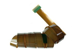
The world of electronics is bending—literally. Flexible printed circuit boards have become the backbone of innovation across industries where traditional rigid boards simply can’t compete. From the intricate sensor arrays in electric vehicles to the life-saving biomedical devices worn on patients’ bodies, flex PCBs enable designs that were once impossible. They fold into smartwatches, curve around camera modules in smartphones, and flex thousands of times inside medical diagnostic equipment without failure.
But here’s the reality that keeps engineers awake at night: a beautifully functional prototype can become a manufacturing disaster when it hits the production floor. The difference between a 95% yield and a 60% yield isn’t just about numbers—it’s about missed deadlines, budget overruns, and the crushing realization that what worked perfectly in your lab fails repeatedly in volume production.
The stakes are particularly high in industries like automotive electronics and medical devices, where flex PCB failures aren’t just inconvenient—they’re potentially catastrophic. An IATF 16949-certified flex PCB for an electric vehicle’s battery management system must withstand constant vibration, thermal cycling, and years of flexing without degradation. An ISO 13485-certified biomedical flex circuit in an implantable device must function flawlessly for the patient’s lifetime.
Most yield-killing mistakes don’t happen on the factory floor. They happen at your desk, during the design phase, weeks or months before the first prototype ever gets fabricated. Understanding these critical pitfalls isn’t just about avoiding problems—it’s about designing for manufacturing excellence from day one.
The Five Mistakes That Destroy Manufacturing Yield
Mistake #1: Ignoring Material Selection for Your Application Environment
Many designers treat material selection as an afterthought, defaulting to standard polyimide constructions without considering the actual operating conditions their flex PCB will face. This single decision cascades through every aspect of manufacturing yield and long-term reliability.
In automotive applications, particularly for electric vehicles, flex PCBs face brutal conditions. A head-up display module experiences temperature swings from -40°C to +125°C, constant vibration from road surfaces, and humidity variations that would destroy inadequately specified materials. Choosing a polyimide film rated for only 105°C might seem like a cost-saving measure during design, but it guarantees delamination failures during thermal cycling tests—long after you’ve committed to tooling and production schedules.
Medical device applications present different but equally demanding challenges. A wearable glucose monitor needs biocompatible coverlay materials that won’t irritate skin during extended wear. The flex circuit in a surgical camera must maintain signal integrity while being repeatedly sterilized. Using standard materials designed for consumer electronics in these applications doesn’t just reduce yield—it creates regulatory compliance nightmares that can derail entire product launches.
The copper foil thickness you specify matters more than most designers realize. Specifying 18μm copper for a flex circuit that needs to survive 100,000 flex cycles in an automated production line is a recipe for copper fatigue and circuit failures. The manufacturing yield might look fine initially, but field failures will appear within months as the copper cracks along bend lines.
Mistake #2: Designing Bend Areas Without Understanding Flex Dynamics
This is where beautiful schematics meet harsh physical reality. Flex PCBs aren’t just thin rigid boards—they’re dynamic structures that experience mechanical stress every time they bend. Designing without accounting for this fundamental difference creates failure points that manufacturing processes can’t overcome.
Sharp 90-degree angles in traces that cross bend areas concentrate stress like a perforation on paper. During assembly, these traces might test perfectly. After 5,000 flex cycles in a smartphone hinge or a medical device actuator, micro-cracks form that progressively increase resistance until the circuit fails. Manufacturing yield looks great, but field reliability collapses.
The bend radius calculation isn’t optional mathematics—it’s physics you can’t negotiate with. A flex PCB stack-up with three copper layers and standard coverlay has a minimum bend radius typically around 10 times the total thickness. Try to fold it tighter, and you’re not creating a more compact design—you’re creating systematic delamination that will show up as manufacturing defects or early field failures. In aerospace applications where flex PCBs route signals through articulating joints, ignoring these calculations means discovering failures during environmental testing, after you’ve invested heavily in the design.
Transition zones between rigid and flexible sections are another minefield. Many designers create abrupt transitions where the rigid board ends and the flex begins, essentially creating a stress concentration point guaranteed to fail. The manufacturing process might successfully produce these boards, but they’ll crack during assembly when components are placed nearby, or fail in the field when the product experiences normal mechanical stress.
Mistake #3: Poor Copper Feature Placement and Trace Routing
Even with perfect materials and bend calculations, how you route traces determines whether your design can be manufactured reliably at volume. Trace placement mistakes are insidious because they often don’t show up in electrical testing—they reveal themselves as intermittent failures or degraded performance that’s maddeningly difficult to diagnose.
Placing traces on the outer layers of a multilayer flex construction that experiences repeated bending is asking for trouble. The outer layers experience the maximum tensile and compressive stress during flexing. In an industrial control application where a flex PCB connects a moving sensor head to a fixed controller, outer-layer traces will fatigue and fail while inner-layer traces remain intact. Smart designers route critical signals on inner layers and use outer layers for less critical connections or leave them as ground/power planes that can tolerate some copper cracking without functional failure.
Straight traces that cross bend lines perpendicular to the bend axis create stress risers that concentrate mechanical forces. The solution—routing traces at 45-degree angles or using curved routing through bend areas—seems simple but requires intentional design work. In telecommunications applications, where flex PCBs route high-speed signals in optical transceiver modules, trace routing mistakes create both mechanical failures and signal integrity problems that devastate yield.
The spacing between traces in flex areas needs to account for copper movement during bending. Traces that are adequately spaced on a rigid board can short together when a flex PCB bends, as the copper deforms slightly and the substrate shifts. This is particularly critical in dense designs for precision smartphone modules where real estate is precious and designers are tempted to pack traces tightly together.
Mistake #4: Inadequate Stack-Up Configuration
The layer stack-up isn’t just about getting signals from point A to point B—it’s a structural design that determines how the flex PCB behaves mechanically. Imbalanced stack-ups create bending bias that causes curling, twisting, and dimensional instability that kills manufacturing yield.
An asymmetric stack-up with heavy copper on one side and light copper on the other creates a bimetallic strip effect. The flex PCB wants to curl toward the heavier copper side, making it difficult to handle during assembly and causing placement accuracy problems. In automotive applications where tight tolerances are critical for connector alignment, this curling can make automated assembly impossible, forcing expensive manual interventions or redesigns.
Layer count decisions affect both electrical performance and mechanical properties. Adding layers to a flex PCB isn’t like adding layers to a rigid board—each additional layer significantly increases stiffness and minimum bend radius. For a wearable medical device that needs to conform to body contours, specifying a four-layer flex when a two-layer design would suffice makes the device uncomfortable to wear and prone to delamination at bend points.
The adhesive versus adhesiveless construction decision impacts everything from flexibility to manufacturing yield. Adhesive-based constructions are generally more economical but create thicker, less flexible circuits with lower heat resistance. Adhesiveless constructions offer better flexibility and thermal performance but cost more and have tighter processing windows. In aerospace applications where weight and reliability are paramount, adhesiveless constructions are often worth the premium despite the manufacturing challenges they introduce.
Mistake #5: Failing to Prototype Under Real-World Conditions
The final critical mistake happens when designers validate their flex PCB designs under lab conditions that bear no resemblance to actual operating environments. A flex PCB that passes all electrical tests while lying flat on a bench might fail catastrophically when installed in the actual product and subjected to real mechanical stress, temperature cycling, and vibration.
Flex testing needs to replicate actual use conditions. For a flex PCB in a laptop hinge that will open and close 50,000 times over the product’s life, you need to test actual flex cycles with the PCB bent to the installed radius, not just bend it by hand a few times. For a medical device flex circuit that experiences repeated sterilization cycles, you need to test after actual autoclave exposure, not just elevated temperature storage.
Environmental testing reveals design weaknesses before they become manufacturing problems. A flex PCB for an electric vehicle charging port needs testing at temperature extremes with real connector mating forces applied. The mechanical stress of connector insertion can cause delamination in poorly designed transition zones that wouldn’t show up in purely electrical testing.
The testing phase is also when you validate assembly processes. Can your flex PCB be reliably assembled using standard SMT equipment, or does it require expensive custom fixturing? Will component placement accuracy meet requirements given the dimensional stability of your flex design? These questions need answers before you commit to volume production.
Strategic Design for Manufacturing Excellence
Understanding what kills yield is only half the battle. The other half is implementing design strategies that actively improve manufacturability and long-term reliability.
Start with design for manufacturing analysis early in the concept phase, not after the design is complete. Engage with your manufacturing partner—whether that’s an in-house team or an external fabricator—to understand their process capabilities and limitations. A manufacturer with advanced equipment might handle designs that would be impossible for others. Flex Plus’s engineering team, for example, works with customers from the initial concept stage, providing DFM analysis that identifies potential yield issues before they’re baked into the design.
Material consultation should be a conversation, not a specification list you copy from a datasheet. Different applications demand different material properties. The polyimide film perfect for a consumer electronics application might be completely wrong for a medical device requiring biocompatibility, or an automotive application requiring IATF 16949 certification. Manufacturers with deep material expertise can guide you toward constructions that meet both functional requirements and manufacturing realities.
Prototyping isn’t just about proving the design works—it’s about validating the entire manufacturing process. Start with small batches that let you identify assembly challenges, test different material options, and validate reliability before committing to production tooling. Rapid prototyping capabilities, like the quick-turn services offered by experienced flex PCB manufacturers, let you iterate quickly and fail fast when failures are cheap to fix.
Testing protocols should mirror real-world use more closely than industry standards often require. Standards provide minimum baselines, but your application might be more demanding. A flex PCB for a drone or eVTOL vehicle experiences vibration profiles that exceed standard automotive testing. Working with a manufacturer who understands these specialized applications means getting test protocols that actually validate real-world reliability.
The relationship between design and manufacturing is a partnership, not a handoff. Designers who treat manufacturing as someone else’s problem create yield nightmares. Manufacturers who don’t provide design feedback miss opportunities to improve customer outcomes. The best results come from collaborative relationships where design and manufacturing expertise combine from day one.
Building Reliability Into Every Layer
Quality doesn’t happen by accident—it’s engineered into every decision from material selection through final assembly. This is where certification standards like ISO 9001, ISO 13485, IATF 16949, and IPC-6013 compliance matter. These aren’t just checkboxes for purchasing departments—they’re systematic quality approaches that reduce variability and improve yield consistency.
For medical device applications, ISO 13485 certification ensures that the flex PCB manufacturer has validated processes for biomedical-compatible materials and maintains the traceability and quality documentation required by regulatory bodies. This systematic approach prevents the kind of material substitutions or process variations that can destroy yield or create field failures in life-critical applications.
In automotive electronics, particularly for electric vehicles, IATF 16949 certification provides confidence that manufacturing processes can maintain the tight tolerances and long-term reliability that vehicle electronics demand. A flex PCB in a battery management system isn’t just another circuit board—it’s a safety-critical component that must function flawlessly for the vehicle’s entire operational life.
The environmental responsibility aspect, represented by ISO 14001 certification, increasingly affects design decisions as customers demand sustainable manufacturing practices. Material choices, waste reduction in the manufacturing process, and end-of-life recyclability considerations are becoming integral to flex PCB design for forward-thinking companies.
From Design to Delivery: The Complete Solution Advantage
The complexity of modern flex PCB applications has created a need for complete solutions that span from initial design consultation through volume production and assembly. Working with manufacturers who offer end-to-end capabilities—from engineering support through fabrication, assembly, and testing—reduces vendor complexity and improves overall outcomes.
Having assembly services integrated with flex PCB fabrication means the team designing your circuit understands exactly how it will be assembled. They can optimize pad layouts for automated placement, specify materials that withstand reflow temperatures, and design test points that work with automated testing equipment. This integration reduces iterations between design, fabrication, and assembly that waste time and money.
Component sourcing integrated with flex PCB manufacturing streamlines supply chain management and reduces delays from parts availability issues. When your flex PCB manufacturer handles component procurement, they can often identify availability problems early and suggest alternatives before you commit to a design that uses hard-to-source components.
Comprehensive testing services ensure that your flex PCBs meet specifications before they reach your assembly line. This includes not just electrical testing but also mechanical testing, environmental testing, and application-specific validation that proves reliability under actual use conditions.
The Path Forward
Designing flex PCBs that deliver high manufacturing yield and long-term reliability isn’t about following a simple checklist—it’s about understanding the deep interconnection between design decisions and manufacturing realities. The five critical mistakes outlined here represent the most common yield killers, but avoiding them requires more than just awareness. It requires partnership with manufacturing experts who can guide design decisions, validate approaches through prototyping, and deliver certified quality in volume production.
The industries driving flex PCB innovation—from electric vehicles and medical devices to aerospace and cutting-edge consumer electronics—demand nothing less than excellence. A head-up display that fails in an electric vehicle creates safety hazards. A wearable medical monitor that fails affects patient health. These aren’t applications where “good enough” suffices.
Working with experienced flex PCB manufacturers who combine advanced technical capabilities with comprehensive certifications provides the foundation for successful designs. Whether you’re developing the next generation of biomedical wearables, designing precision modules for telecommunications infrastructure, or creating innovative solutions for emerging industries like eVTOL vehicles and beauty tech, your flex PCB design decisions made today determine your product’s success tomorrow.
The most successful engineers don’t just design circuits—they design for manufacturing excellence from the very first schematic capture. They understand that yield isn’t just a manufacturing metric—it’s a design outcome. By avoiding these five critical mistakes and partnering with manufacturers who bring both technical expertise and certified quality processes to the table, you can create flex PCB designs that work brilliantly in the lab and scale flawlessly to volume production.
Because in the end, the best flex PCB design isn’t the one with the most elegant schematic or the tightest trace routing—it’s the one that consistently delivers 95%+ yields in manufacturing while meeting every reliability requirement in the field. That’s the standard that drives innovation forward and turns great designs into successful products.