
Flexible printed circuit boards have become the backbone of modern electronics, powering everything from medical implants to electric vehicle displays. As industries push toward miniaturization and enhanced functionality, the demand for flexible PCBs continues to surge. However, designing these intricate circuits requires more than just technical knowledge—it demands a deep understanding of critical parameters that directly impact performance, durability, and manufacturability.
At Flex Plus (Xiamen) Co., Ltd, we’ve witnessed countless engineers face challenges during production simply because they overlooked fundamental flex circuit design guidelines. After serving over 2,500 customers across diverse industries for more than 20 years, we’ve identified seven critical parameters that every engineer must master before moving to production. Understanding these rules doesn’t just prevent costly redesigns—it unlocks the full potential of flexible PCB technology.
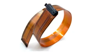
Understanding Bend Radius: The Foundation of Flexible Design
The bend radius is arguably the most critical parameter in flexible PCB design. It defines the minimum radius to which a flexible circuit can bend without sustaining damage to its copper traces, substrate, or laminate structure. Ignoring this parameter is like building a bridge without calculating load capacity—failure is inevitable.
The formula for calculating minimum bend radius is straightforward: R = T × N, where R represents the bend radius, T is the total thickness of the flexible circuit, and N is a multiplier that varies based on application. For static applications where the circuit bends once during installation and remains fixed, a multiplier of 6-10 times the thickness is generally acceptable. However, dynamic applications—where the circuit flexes repeatedly during operation—require a more conservative approach with multipliers ranging from 15-20 times or even higher.
Consider a double-sided flexible circuit with a total thickness of 0.5mm. For static use, a bend radius of 5mm (10 × 0.5mm) provides adequate safety. But if that same circuit operates in a dynamic environment like a smartphone hinge or a robotic arm joint, the bend radius should increase to at least 10mm to ensure longevity.
Real-world consequences of inadequate bend radius are severe. A leading consumer electronics manufacturer once approached us after their in-house designed flexible circuits failed prematurely in their foldable smartphone prototypes. The investigation revealed that their bend radius was merely 4 times the circuit thickness—far below the recommended range for dynamic flexing. The result? Cracked copper traces, delamination, and complete circuit failure within 10,000 flex cycles. After redesigning with proper bend radius calculations, their flex life exceeded 200,000 cycles.
When designing your flexible PCB, avoid sharp 90-degree angles in bend areas. Instead, incorporate smooth, gradual curves that distribute mechanical stress evenly, following proven design guidelines that prevent manufacturing nightmares. Position traces perpendicular to the bend axis whenever possible, and never place vias directly in flex zones. These simple guidelines, combined with proper bend radius calculations, form the foundation of reliable flexible circuit design.
Maximizing Flex Life: Engineering for Durability
Flex life refers to the number of times a flexible circuit can bend and return to its original position before experiencing electrical or mechanical failure. This parameter directly determines product lifespan in applications ranging from laptop hinges to medical wearables, making it crucial for engineers designing dynamic flexible circuits.
Several factors influence flex life, with material selection playing a primary role. Polyimide substrates consistently outperform polyester alternatives in dynamic applications due to superior tear resistance and thermal stability. At Flex Plus, our ISO 13485-certified manufacturing processes utilize high-grade polyimide materials that maintain integrity through hundreds of thousands of flex cycles, essential for biomedical devices where failure isn’t an option.
Copper foil type significantly impacts flex life as well. Rolled annealed copper offers exceptional flexibility compared to electrodeposited copper, as its grain structure aligns with the rolling direction, reducing crack propagation during repeated flexing. When designing for high flex life applications, specifying rolled copper in your stackup isn’t just recommended—it’s essential.
Trace routing strategy directly correlates with flex life performance. Engineers should route traces parallel to the bend axis rather than perpendicular, minimizing stress concentration. Additionally, positioning copper on the neutral axis of the flexible substrate—the centerline where neither compression nor tension occurs during bending—dramatically extends flex life. This principle guides our multilayer flexible PCB designs at Flex Plus, where we strategically balance copper layers around the neutral axis to optimize mechanical performance.
A medical device manufacturer partnered with us to develop a flexible circuit for a wearable cardiac monitor. Their initial design routed traces perpendicular to the primary bend axis, resulting in failures after just 50,000 cycles—far short of their 500,000-cycle requirement. By reorienting traces parallel to bending, incorporating rolled copper, and optimizing the neutral axis placement, we achieved over 750,000 cycles in testing, exceeding their expectations and ensuring patient safety.
Temperature cycling also affects flex life. Flexible circuits operating in environments with significant temperature fluctuations experience coefficient of thermal expansion (CTE) mismatches between materials, accelerating fatigue. Conducting thorough thermal analysis during the design phase helps identify potential weaknesses before production, saving both time and resources.
Accounting for Dynamic Stress: Anticipating Real-World Conditions
Dynamic stress encompasses the mechanical forces flexible circuits experience during operation—bending, twisting, vibration, and tension. Unlike rigid PCBs that remain stationary, flexible circuits must maintain electrical integrity while withstanding continuous mechanical deformation. Failing to account for dynamic stress leads to premature failures that frustrate customers and damage brand reputation.
Engineers must recognize that stress concentrates at specific points within flexible circuits. Transition zones between rigid and flexible sections experience the highest stress levels, as material properties change abruptly. Sharp corners, tight bend radii, and areas with high component density also become stress concentration points that require special attention.
One effective strategy involves incorporating stiffeners at rigid-to-flex transition zones. These stiffeners—typically polyimide or FR4 material—gradually transition the mechanical properties between sections, distributing stress more evenly. At Flex Plus, our rigid-flex PCB capabilities include precision stiffener placement optimized through finite element analysis (FEA), ensuring smooth stress distribution across the entire assembly. At Flex Plus, our rigid-flex PCB capabilities include precision stiffener placement optimized through finite element analysis (FEA), ensuring smooth stress distribution across the entire assembly.
Component placement significantly influences dynamic stress performance. Placing components directly in flex zones subjects them to continuous mechanical stress, causing solder joint failures and component cracking. Best practice dictates mounting components exclusively in rigid sections or areas with stiffener reinforcement. When components must exist near flex zones, leaving adequate clearance—typically 3-5mm—from the actual flex area provides necessary protection.
An automotive electronics manufacturer designing head-up display circuits for electric vehicles learned this lesson the hard way. Their initial design placed several SMD components within 1mm of a dynamic flex zone. During vibration testing simulating real-world driving conditions, solder joints failed within 500 hours—unacceptable for IATF 16949 certification requirements. Relocating components to reinforced areas and increasing clearance from flex zones resulted in zero failures during 2000-hour extended testing, meeting strict automotive reliability standards.
Implementing teardrop pad designs at via connections reduces stress concentration points. Standard circular pads create sharp transition points where traces meet vias, but teardrop shapes provide gradual transitions that better withstand dynamic stress. This simple design modification significantly enhances reliability without increasing manufacturing complexity.
Managing Temperature: Thermal Considerations in Flexible Design
Temperature management represents a critical yet often overlooked parameter in flexible PCB design. Unlike rigid boards with substantial thermal mass, flexible circuits have limited ability to dissipate heat, making them vulnerable to thermal degradation. Understanding how temperature affects material properties and electrical performance is essential for creating reliable designs.
Polyimide substrates maintain excellent mechanical properties at elevated temperatures, typically rated for continuous operation up to 200°C. However, sustained exposure to temperatures near these limits accelerates aging processes, reducing flex life and electrical performance over time. Copper oxidation increases at elevated temperatures, potentially compromising trace conductivity and adhesion to the substrate.
Adhesive systems deserve special attention in thermal management. Acrylic adhesives, while cost-effective, begin degrading around 105°C, limiting their application in high-temperature environments. Polyimide-based adhesive systems offer superior thermal stability, maintaining integrity beyond 200°C—essential for applications like EV battery management systems or industrial control equipment operating in harsh conditions.
At Flex Plus, we’ve developed innovative solutions for thermal challenges, including flexible heat dissipation flow channels that actively manage heat in high-power applications. This breakthrough technology allows flexible circuits to handle thermal loads previously impossible, opening new possibilities for power electronics and LED lighting applications.
Temperature cycling presents another challenge. When flexible circuits operate across wide temperature ranges—common in automotive and aerospace applications—CTE mismatches between materials create mechanical stress that compounds with dynamic flexing. A circuit operating from -40°C to +125°C experiences significant dimensional changes as materials expand and contract at different rates. Selecting materials with matched CTE properties minimizes this stress, improving long-term reliability.
A telecommunications equipment manufacturer designing optical transceiver modules faced thermal challenges when their flexible interconnects failed during temperature cycling tests. Analysis revealed that standard acrylic adhesive degraded under repeated thermal stress. Switching to polyimide adhesive systems and optimizing copper thickness to reduce thermal expansion stress resolved the failures, enabling their modules to pass rigorous telecommunications industry standards.
Thermal modeling during the design phase identifies potential hot spots before production. Modern simulation tools analyze heat distribution across flexible circuits, allowing engineers to optimize trace widths, copper weights, and component spacing for improved thermal performance. This proactive approach prevents costly redesigns and accelerates time-to-market.
Selecting Materials: Building Blocks of Flexible Excellence
Material selection fundamentally determines flexible PCB performance, influencing everything from flex life to thermal stability to chemical resistance. Understanding the properties and applications of different materials empowers engineers to make informed decisions that optimize both performance and cost.
Polyimide film serves as the gold standard for flexible circuit substrates. Its exceptional thermal stability, mechanical strength, and chemical resistance make it ideal for demanding applications. Standard polyimide films like DuPont Kapton or similar materials maintain properties across temperature ranges from -269°C to +400°C, though practical applications typically operate between -40°C and +200°C. The material’s excellent dimensional stability ensures consistent electrical performance even under thermal cycling.
Polyester (PET) substrates offer a cost-effective alternative for less demanding applications. While limited to lower operating temperatures—typically below 105°C—polyester provides adequate performance for consumer electronics, simple sensors, and applications without severe thermal or mechanical stress. Understanding the fundamental properties of materials helps engineers make informed substrate selection decisions. A fitness tracker manufacturer, for instance, successfully utilized polyester-based flexible circuits in their entry-level products, achieving significant cost savings while maintaining acceptable reliability for the product’s intended lifespan.
Copper foil selection impacts both electrical and mechanical performance. Rolled annealed (RA) copper provides superior flexibility and elongation properties compared to electrodeposited (ED) copper, making it the preferred choice for dynamic applications. ED copper, while less flexible, offers finer feature resolution capabilities beneficial for high-density interconnect designs in smartphones and wearables. At Flex Plus, we offer copper foil options ranging from 18μm to 70μm, allowing precise optimization for each application’s requirements.
Adhesive systems constitute another critical material choice. Traditional acrylic adhesives provide good initial adhesion and cost advantages but limit thermal performance. Epoxy adhesives offer improved thermal and chemical resistance but sacrifice some flexibility. Polyimide adhesive systems deliver the best overall performance, maintaining properties at elevated temperatures while preserving flexibility—ideal for aerospace, medical, and automotive applications where reliability cannot be compromised.
Adhesiveless constructions represent the pinnacle of flexible PCB technology. By directly laminating copper to polyimide through specialized processes, these circuits eliminate adhesive layers entirely, reducing thickness, improving flexibility, and enhancing thermal performance. Our ultra-thin flexible PCB capabilities at Flex Plus achieve overall thickness as low as 25 microns with gold plating on double-sided designs—enabling applications previously impossible with conventional flexible circuits.
Coverlay materials protect circuits from environmental exposure and provide electrical insulation. Polyimide coverlay with acrylic or epoxy adhesive offers excellent protection while maintaining flexibility. For applications requiring solder mask instead, photoimageable solder masks designed specifically for flexible circuits provide fine-feature definition without compromising flexibility.
Optimizing Copper Features: Trace Routing and Pad Design
Copper feature design directly impacts both electrical performance and mechanical reliability in flexible PCBs. Proper trace routing, pad design, and via placement distinguish successful designs from problematic ones, affecting everything from signal integrity to flex life.
Trace width and spacing require careful consideration in flexible designs. While minimum capabilities might reach 2mil/2mil (50μm/50μm) in advanced manufacturing facilities like Flex Plus, practical designs should incorporate wider traces whenever possible to improve both electrical performance and mechanical reliability. Wider traces better withstand flexing stresses and provide lower resistance for power distribution.
Trace routing orientation relative to bend axes critically affects reliability. Traces running perpendicular to the bend axis experience maximum stress during flexing, while parallel traces distribute stress more evenly along their length. When perpendicular routing becomes unavoidable, using curved rather than straight traces and increasing trace width in flex zones compensates for the adverse orientation.
Avoiding sharp angles in trace routing is essential for flexible circuits. Right-angle turns create stress concentration points that accelerate crack formation during flexing. Instead, engineers should implement smooth curves with gradual transitions—think of designing roads rather than city grid patterns. This approach not only improves mechanical reliability but also reduces signal reflection in high-frequency applications.
Pad design influences both assembly reliability and mechanical performance. Standard circular pads create abrupt transitions where traces connect, concentrating stress at these junctions. Teardrop pad designs provide gradual transitions that distribute stress over a larger area, significantly improving resistance to fatigue cracking. This simple modification costs nothing in terms of board area yet delivers substantial reliability improvements.
Via placement demands special attention in flexible PCB design. Vias represent discontinuities in the flexible structure, creating stress concentration points. Placing vias directly in flex zones invites premature failure as repeated bending causes plating cracks and eventual electrical opens. Best practice dictates keeping vias in rigid sections or reinforced areas, maintaining at least 1-2mm clearance from actual flex zones.
Staggered via patterns provide superior mechanical performance compared to inline arrangements. When vias must exist near flex zones, offsetting them distributes stress more evenly across the substrate rather than creating a linear weak point. This technique, combined with teardrop pad designs, maximizes via reliability in challenging applications.
An industrial automation customer designing control system interconnects initially struggled with via failures in their flexible circuits. Their design featured rows of vias aligned parallel to flex zones, creating linear stress concentration points. Redesigning with staggered via patterns and increased clearance from flex zones eliminated failures, achieving zero field returns over two years of production—a dramatic improvement from their original 3% failure rate.
Copper balancing across layers improves mechanical symmetry in multilayer flexible circuits. Asymmetric copper distribution causes circuits to curl or warp, affecting assembly and potentially creating stress during flexing. Balancing copper features between layers—even adding dummy copper fills when necessary—maintains dimensional stability and improves overall reliability.
Balancing Electrical and Mechanical Requirements
Successful flexible PCB design requires simultaneously satisfying electrical and mechanical requirements—a balancing act that challenges even experienced engineers. Electrical considerations like impedance control, signal integrity, and power distribution often conflict with mechanical needs such as flexibility, bend radius, and stress distribution. Achieving optimal balance requires holistic thinking and iterative optimization.
Impedance control in flexible circuits presents unique challenges compared to rigid boards. The thinner dielectric layers and material property variations in flexible substrates affect impedance calculations. Engineers must account for how bending influences dielectric thickness and material properties, potentially shifting impedance during operation. Using impedance modeling tools specifically calibrated for flexible materials helps maintain signal integrity across operational conditions.
Layer stackup design fundamentally affects both electrical and mechanical performance. Positioning copper layers symmetrically around the neutral axis optimizes mechanical properties while allowing sufficient dielectric thickness for impedance control. Our ISO 9001-certified design processes at Flex Plus incorporate comprehensive stackup analysis that balances these competing requirements, ensuring designs perform reliably in both domains.
Ground plane implementation illustrates the electrical-mechanical tradeoff clearly. Solid ground planes provide excellent EMI shielding and signal return paths but significantly reduce flexibility. Hatched or crosshatch ground patterns maintain acceptable electrical performance while preserving mechanical flexibility—a compromise often necessary in dynamic applications. The pattern density requires optimization based on frequency requirements and flexibility needs.
Power distribution networks in flexible circuits must balance current carrying capacity with flexibility requirements. Wide power traces improve conductivity and reduce voltage drop but stiffen the circuit. Breaking wide traces into multiple parallel narrower traces maintains current capacity while preserving flexibility—a technique particularly valuable in power-sensitive applications like EV systems.
A beauty tech manufacturer developing flexible circuits for innovative hair styling devices faced this exact challenge. Their design required 3A current capacity through flex zones while maintaining sufficient flexibility for user manipulation. Standard approaches with wide power traces created unacceptably stiff circuits. By implementing multiple parallel 0.5mm traces instead of single 1.5mm traces, we achieved equivalent current capacity while preserving the flexibility their industrial design demanded.
Component placement decisions significantly impact the electrical-mechanical balance. While concentrating components minimizes board size and improves electrical performance through shorter traces, it increases weight and stiffness that compromise mechanical properties. Strategic component distribution—placing heavier components in reinforced areas while keeping flex zones light—optimizes both aspects.
Thermal management intersects both electrical and mechanical domains. Electrical losses generate heat that flexible circuits must dissipate despite limited thermal mass. Mechanical flexing generates localized heating through material hysteresis. Engineers must consider both heat sources when designing thermal management strategies, potentially incorporating heat spreaders, thermal vias, or specialized materials.
Controlling Costs Through Design Optimization
Cost considerations profoundly influence flexible PCB design decisions. While achieving technical performance remains paramount, optimizing designs for manufacturability directly impacts project economics and commercial viability. Understanding cost drivers empowers engineers to make informed design decisions that balance performance, reliability, and affordability.
Material selection represents the most significant cost variable in flexible PCB manufacturing. Polyimide substrates cost substantially more than polyester alternatives, but their superior properties justify the premium for demanding applications. Engineers should honestly assess whether applications truly require polyimide’s capabilities or if polyester suffices—using premium materials only where necessary rather than defaulting to them universally.
Layer count dramatically affects manufacturing complexity and cost. Each additional layer increases processing steps, material costs, and yield risks. While multilayer designs enable compact layouts and improved electrical performance, designers should critically evaluate whether functionality truly requires multiple layers or if clever single or double-sided designs achieve equivalent results. At Flex Plus, we’ve helped numerous customers reduce layer counts through creative design optimization, cutting costs by 30-40% without compromising functionality.
Feature sizes influence manufacturing yield and cost. Pushing minimum line width/spacing capabilities to extremes increases defect rates and requires specialized processing that elevates costs. Designing with relaxed geometries—perhaps 4mil/4mil instead of 2mil/2mil—improves manufacturability and reduces costs while still meeting most applications’ electrical requirements. Reserve fine features for areas where absolutely necessary rather than applying them across entire designs.
Panel utilization optimization maximizes the number of circuits produced per manufacturing panel, directly reducing per-unit costs. Working with manufacturers during the design phase to optimize circuit dimensions and array configurations improves panel efficiency. Seemingly minor dimension changes—perhaps adjusting a circuit from 53mm to 50mm width—might enable fitting additional circuits per panel, significantly reducing per-unit costs in volume production.
Standardizing designs across product families reduces engineering and tooling costs. Developing flexible platform designs that accommodate multiple product variants through minor modifications leverages development investments across broader product lines. This approach, commonly used in smartphone manufacturing, significantly reduces development costs while maintaining product differentiation.
An electric vehicle manufacturer partnered with Flex Plus to develop flexible circuits for their display systems. Their initial design used polyimide throughout, including areas experiencing no thermal or mechanical stress. By substituting polyester in non-critical sections while maintaining polyimide in high-stress zones, we reduced material costs by 25% without compromising reliability in actual operating conditions. This hybrid approach exemplifies intelligent cost optimization that maintains performance where critical while economizing elsewhere.
Quick-turn prototyping capabilities enable cost-effective design iteration. Rather than committing to full production with unproven designs, investing in rapid prototypes validates concepts and identifies issues early when modifications cost least. Partnering with an experienced flexible PCB supplier ensures access to these critical prototyping services. At Flex Plus, our 1-week standard prototyping turnaround—3 days for emergency requests—enables iterative optimization that prevents costly production redesigns.
Assembly considerations impact total product cost beyond just board fabrication. Designing for automated assembly reduces labor costs and improves consistency. Standardizing component packages, maintaining adequate spacing for pick-and-place equipment, and incorporating alignment features facilitates efficient assembly. Our comprehensive flex PCBA services reduce vendor count and streamline production, eliminating coordination overhead while ensuring quality through single-source accountability.
Conclusion: Excellence Through Comprehensive Understanding
Mastering these seven critical parameters—bend radius, flex life, dynamic stress, temperature management, material selection, copper feature optimization, and cost considerations—transforms good engineers into exceptional flexible PCB designers. Success requires viewing these parameters not in isolation but as interconnected aspects of holistic design that simultaneously addresses electrical, mechanical, thermal, and economic requirements.
At Flex Plus (Xiamen) Co., Ltd, two decades of flexible PCB manufacturing experience across diverse industries from medical devices to electric vehicles has taught us that excellence emerges from comprehensive understanding. Our ISO-certified manufacturing processes, advanced COB integration capabilities, and engineering partnership approach reflect a commitment to not just building circuits but enabling innovation through superior flexible solutions.
Whether you’re developing cutting-edge beauty tech gadgets, autonomous drone systems, or life-saving medical devices, these fundamental design rules provide the foundation for reliable, manufacturable flexible circuits. Combined with expert manufacturing partners who understand both the technical requirements and practical realities of production, they enable you to transform ambitious concepts into commercial reality.
The flexible PCB industry continues evolving with ever-increasing demands for higher density, greater reliability, and improved performance. By internalizing these critical parameters and applying them systematically throughout your design process, you position yourself to meet these challenges successfully—creating flexible circuits that don’t just function but excel in their intended applications.
From design consultation through prototyping to full-scale production and assembly, partnering with experienced manufacturers committed to engineering excellence ensures your flexible PCB designs achieve their full potential. The investment in understanding and properly implementing these seven critical parameters pays dividends throughout product lifecycles, reducing failures, improving customer satisfaction, and ultimately defining the difference between adequate performance and exceptional success.