
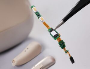
In a world where technology constantly shrinks while growing more powerful, an unsung hero works behind the scenes: high density interconnect flexible circuits. These remarkable components have revolutionized how we design and build everything from smartphones to medical implants, enabling the sleek, feature-packed devices we’ve come to rely on daily.
As our devices get smaller, thinner, and more capable, manufacturers face increasing challenges to pack more functionality into diminishing spaces. This is where high density interconnect (HDI) flexible circuits shine, offering an elegant solution that supports innovation across electric vehicles, medical devices, wearables, telecommunications equipment, and countless other applications.
The Miniaturization Revolution
The demand for miniaturization has driven significant advancements in electronic design. Today’s smartphones contain computing power that would have filled entire rooms just decades ago. Medical devices that once required bulky equipment can now be worn on the body or even implanted. Electric vehicles integrate sophisticated control systems within tight spaces. This transformation wouldn’t be possible without high density interconnect flexible circuits.
These specialized circuits allow designers to create interconnections at a density previously unimaginable, using materials that can bend, fold, and flex without sacrificing functionality. The result? Devices that are not only smaller but also lighter, more reliable, and capable of fitting into previously impossible spaces or conforming to unusual shapes.
The market for HDI flexible circuits has seen remarkable growth, with recent reports showing a surge in demand of over 10% annually. This growth is driven by industries requiring cutting-edge solutions in an increasingly AI-dominated landscape, where processing power and connectivity demands continue to escalate.
Key Features of HDI Flexible Circuits
What makes high density interconnect flexible circuits so special? Several critical innovations set them apart from traditional printed circuit boards:
Microvias: Tiny Connections, Enormous Impact
Microvias are extremely small holes (typically under 150 micrometers in diameter) that create connections between layers in a circuit. These minuscule pathways allow for significantly higher connection density than traditional through-holes. Using advanced techniques like laser direct drilling, manufacturers can create precise, reliable connections in incredibly tight spaces.
Today’s advancements in formulations and equipment have made direct metallization the preferred choice for fabricating microvias in flexible and rigid HDI PCBs. This process creates more reliable connections while reducing manufacturing steps.
Fine-Pitch Components
HDI flexible circuits support components with extremely fine pitch (the distance between connection points). Modern HDI designs can accommodate components with pitches as small as 0.4mm or less, allowing for the integration of advanced processors, memory, and other sophisticated components in tight spaces.
The ability to work with fine-pitch components is crucial for applications like smartphone camera modules, medical imaging devices, and automotive sensor systems where space is at an absolute premium.
Advanced Layering Techniques
High density interconnect flexible circuits employ sophisticated layering strategies that maximize space efficiency. Unlike conventional PCBs, HDI flexible circuits can utilize:
– Staggered vias
– Stacked vias
– Blind and buried vias
– Sequential build-up processes
These techniques allow designers to create complex routing solutions in extremely compact designs, often with 4-8 layers in spaces where traditional boards might require twice that number.
Flexible Materials
Perhaps most importantly, these circuits are built on flexible substrate materials, typically polyimide, which can bend and flex without breaking. This flexibility enables:
– 3D design possibilities that rigid boards cannot achieve
– Elimination of connectors and cables
– Reduction in overall weight and size
– Greater durability against vibration and movement
– Improved thermal management through novel configurations
The combination of flexibility with high-density connections creates unique possibilities for products that need to fit into small, oddly shaped spaces or withstand physical strain. This is particularly valuable in wearable technology, where devices must conform to the human body while maintaining electronic performance. Flexible PCB materials play a critical role in enabling this adaptability.
Advanced Design Strategies for HDI Flexible Circuits
Creating effective high density interconnect flexible circuits requires sophisticated design approaches that go beyond traditional PCB methodologies. Engineers must carefully consider several factors:
Optimal Layer Configuration
The stack-up of an HDI flexible PCB demands careful planning. Engineers must intelligently arrange copper layers, prepreg, and dielectrics to maximize wiring density and signal integrity. This often involves asymmetric designs that place critical signal layers where they can be most effective.
A critical design tip: avoid placing vias, pads, or components within bend areas to reduce the risk of mechanical failure. Minimizing the number of layers in a bend area significantly improves reliability over the product’s lifespan.
Routing Efficiency
With space at such a premium, efficient routing becomes essential. Advanced HDI designs incorporate techniques like:
– Microvias (as small as 0.004″ diameter) to create dense connection patterns
– Cross-hatched ground planes that maintain electrical performance while enhancing flexibility
– Careful signal path planning to minimize length and crossover
– Zone-based design approaches that separate rigid and flexible areas
These routing strategies enable designers to achieve remarkable space efficiency without compromising signal integrity or manufacturing yield.
Thermal Management
As components pack more tightly together, heat dissipation becomes increasingly challenging. Innovative HDI flexible circuit designs incorporate thermal management solutions such as:
– Flexible heat dissipation flow channels
– Copper coin technology for hotspot management
– Strategic ground plane designs that help distribute heat
– Materials with enhanced thermal conductivity
These thermal strategies are particularly important in applications like electric vehicle control systems and high-performance computing devices where heat can significantly impact performance and reliability.
Rigorous Testing Protocols
HDI flexible circuits require comprehensive testing to ensure reliability. Leading manufacturers implement:
– Automated optical inspection (AOI) for microscopic defects
– Electrical testing for continuity and isolation
– Bend and flex testing to verify mechanical durability
– Environmental stress testing to ensure performance in real-world conditions
These testing protocols help ensure that the finished products will maintain reliability even under challenging operating conditions.
Cutting-Edge HDI Flexible Circuit Solutions
At Flex Plus (Xiamen) Co., Ltd., a leading certified flexible PCB manufacturer since 2004, advanced high density interconnect flexible circuits have been at the core of our innovation strategy. Our approach combines cutting-edge manufacturing techniques with deep engineering expertise to create solutions that push the boundaries of what’s possible.
The company’s HDI flexible circuit capabilities include precision manufacturing with line width/spacing as fine as 2/2mil, layer counts from 1-8 layers, and advanced quick-turn prototyping services. This precision enables the creation of ultra-thin designs—some as thin as 25 microns with gold plating on double-sided flex PCBs—a critical capability for next-generation applications.
Unlike PCB brokers or trading companies, Flex Plus maintains complete manufacturing control with an 8,000+ square meter factory equipped with advanced production lines. This manufacturing excellence translates into high-quality, reliable HDI flexible circuit solutions that meet rigorous international standards, including ISO 9001, ISO 13485, and IATF 16949 certifications.
Real-World Applications Across Industries
High density interconnect flexible circuits are transforming products across diverse industries:
In electric vehicles, HDI flexible circuits enable sophisticated head-up displays, wing mirror controls, side cameras, parking sensors, and Lidar systems—all of which must fit into constrained spaces while maintaining reliability under harsh automotive conditions.
Medical device manufacturers leverage HDI flexible circuits to create biomedical-compatible devices that can conform to the human body or fit within tiny implantable packages, all while maintaining ISO 13485 certification standards.
In the emerging low-altitude airspace market, drones, eVTOL vehicles, and aerial logistics systems rely on lightweight, reliable HDI flexible circuits to maximize payload capacity while ensuring control system integrity.
Beauty tech companies integrate HDI flexible circuits into tech-driven beauty gadgets, creating products that combine sophisticated electronics with ergonomic designs that users find comfortable and intuitive.
For augmented reality wearables and AI glasses, ultra-thin HDI flexible circuits make possible comfortable, lightweight devices that can process complex visual data without bulky components

The Future of HDI Flexible Circuit Technology
As we look toward the future, high density interconnect flexible circuit technology continues to advance rapidly. Several emerging trends promise to further revolutionize electronic design:
Advancements in materials science are yielding substrates with even greater flexibility, temperature resistance, and reliability. These new materials will enable HDI flexible circuits to function in increasingly challenging environments.
Manufacturing innovations like laser direct imaging are improving accuracy and reducing production time for complex HDI designs, making these sophisticated components more accessible to a wider range of products.
Integration with advanced packaging technologies, particularly Chip-on-Board (COB) solutions, is creating new possibilities for ultra-compact, high-performance electronic modules. Flex Plus has pioneered flexible substrate COB technology with remarkable precision—achieving wafer offset angle tolerance controlled within ±5° and micron-level packaging with thickness tolerance within 50-100μm.
The continued growth of AI and interconnected devices will further drive demand for HDI flexible circuits that can support high-speed data transmission in compact packages, particularly in telecommunications and edge computing applications.
Conclusion
High density interconnect flexible circuits represent a remarkable achievement in electronic design—a technology that continues to evolve and enable innovation across countless industries. From the smartphone in your pocket to the medical device saving lives to the electric vehicle reducing carbon emissions, these hidden components make modern technology possible.
As devices continue to shrink while growing more powerful, the importance of high density interconnect flexible circuits will only increase. Companies at the forefront of this technology, like Flex Plus (Xiamen) Co., Ltd., with its commitment to quality, innovation, and comprehensive manufacturing capabilities, will continue driving progress in this vital field.
The next time you marvel at the sleek design of your latest gadget, remember the sophisticated high density interconnect flexible circuits inside, silently enabling the technology that enriches our daily lives.