
In the ever-evolving landscape of modern electronics, few advancements have proven as transformative as Chip on Board (CoB) technology. This revolutionary approach to component integration represents a fundamental shift in how electronic devices are designed, manufactured, and optimized for performance. By directly mounting bare semiconductor chips onto a printed circuit board substrate, CoB technology eliminates traditional packaging, dramatically reducing the size and weight of electronic components while enhancing their functionality and reliability.
The significance of CoB technology is particularly evident in industries where space constraints, weight considerations, and performance demands converge. Electric vehicle manufacturers leverage this technology to create lighter, more efficient control systems. Medical device companies employ CoB to develop smaller, more reliable implantable devices and diagnostic equipment. Telecommunications equipment providers utilize it to pack more functionality into transmission modules and network infrastructure. As devices continue to shrink while capabilities expand, flexible chip on board technology stands at the forefront of this miniaturization revolution.
Advantages of CoB Integration: Precision Meets Performance
The marriage of CoB technology with flexible substrates creates a powerhouse of advantages that extend far beyond simple space savings. This integration offers substantial cost benefits throughout the production process. By eliminating the need for separate IC packaging, manufacturers can reduce component costs, streamline assembly processes, and minimize material waste. These efficiency gains translate directly to competitive pricing without compromising quality or performance.
Perhaps more importantly, flexible chip on board integration delivers remarkable performance improvements. The direct bonding of chips to substrates significantly reduces signal path lengths, minimizing parasitic capacitance and inductance that can degrade signal integrity. This direct connection enables faster signal transmission, reduced power consumption, and enhanced thermal management – critical factors in high-performance applications.
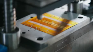
At the heart of these performance gains lies the breakthrough ±5° precision bonding technology. This exceptional level of accuracy ensures perfect alignment between chips and substrates, maintaining consistent electrical connections even under mechanical stress or thermal cycling. Such precision is essential for industries requiring high-reliability PCBs, such as aerospace systems, defense equipment, and industrial control networks where failure is simply not an option.
““Achieving ±5° precision bonding on flexible substrates represents a quantum leap in manufacturing capability,”” explains an industry expert. “This tolerance level ensures operational stability under conditions that would cause traditional solutions to fail, opening new possibilities for where and how electronic systems can be deployed.”
Transforming Electronic Designs Through Flexibility and Innovation
The true revolution of flexible chip on board technology lies in its ability to transform how we conceptualize electronic designs. Traditional rigid PCBs impose significant constraints on product development, forcing designers to adapt their visions to the limitations of the technology. Flexible CoB liberates this creative process, enabling electronics to conform to product requirements rather than the reverse.
This transformative approach is particularly evident in smartphone module development. The latest generation of phones incorporates curved displays, folding screens, and complex internal geometries that would be impossible with conventional rigid components. Flexible CoB enables camera modules, sensors, and processing units to fit into previously unusable spaces, maximizing functionality while maintaining sleek form factors.
In the wearable technology sector, flexible chip on board has catalyzed an explosion of innovation. Smart watches, fitness trackers, and medical monitoring devices benefit from components that can conform to the human body. These devices can now bend, twist, and flex with natural movement while maintaining perfect functionality – a direct result of the stability provided by precision bonding techniques.
Perhaps most exciting is the application in low-altitude airspace innovations. Drones, electric vertical takeoff and landing (eVTOL) vehicles, and aerial logistics platforms require extremely lightweight yet robust electronic systems that can withstand vibration and acceleration. Flexible CoB provides the ideal solution, delivering computing power and sensor capabilities in packages that weigh mere grams rather than ounces.
Materials and Techniques: The Building Blocks of Miniaturization
The remarkable capabilities of flexible chip on board technology stem from sophisticated materials and manufacturing techniques that push the boundaries of what’s possible in electronics fabrication.
At the foundation of this technology is the flexible substrate itself. Unlike traditional rigid FR-4 materials, flexible substrates typically utilize polyimide films that offer exceptional thermal stability, chemical resistance, and dimensional control even at thicknesses below 50 micrometers. These materials maintain their electrical and mechanical properties through hundreds of thousands of flexing cycles, ensuring long-term reliability in dynamic applications.
Gold plating plays a crucial role in the performance and reliability of flexible CoB systems. Unlike solder-based connections that can crack under repeated flexing, gold bonding wires and pads maintain consistent electrical performance through temperature extremes and mechanical stress. The corrosion resistance of gold ensures that these critical connections remain stable throughout the product lifecycle, even in harsh environments.
A key technical consideration in flexible CoB design is the avoidance of via holes in the immediate vicinity of chips. These holes, which traditionally provide electrical connections between layers, can create stress points that compromise the integrity of the delicate bonds between chips and substrates. Advanced designs utilize strategic routing techniques that maintain signal integrity while eliminating these potential failure points.
““The material science behind flexible chip on board is as impressive as the electrical engineering,”” notes a leading R&D engineer. “Creating substrates that can maintain dimensional stability to micrometer tolerances while remaining flexible enough for real-world applications requires pushing materials to their theoretical limits.”
These technical considerations resonate particularly with precision electronics designers and R&D engineers seeking customized solutions. The ability to achieve component densities previously thought impossible, while maintaining the flexibility to conform to three-dimensional spaces, opens new avenues for innovation across countless applications.
Real-World Applications: From Beauty Tech to Augmented Reality
The impact of flexible chip on board technology extends far beyond theoretical advantages, finding practical applications across an increasingly diverse range of industries.
In the rapidly growing beauty tech sector, flexible CoB has enabled a new generation of smart skincare devices. These products incorporate advanced sensors that analyze skin condition, microprocessors that adjust treatment parameters, and precision actuators that deliver active ingredients – all in handheld devices that conform to facial contours. The miniaturization made possible by flexible chip on board allows these devices to maintain elegant, non-intimidating designs while delivering clinical-grade performance.
Smart helmet technology represents another compelling application. Modern F1 racing helmets integrate impact sensors, communication systems, and heads-up displays without adding bulk or weight that could compromise driver safety. In mining and mineral extraction, similar helmets monitor environmental conditions, worker vital signs, and potential hazards while withstanding the demanding conditions of underground operations. Flexible CoB makes these capabilities possible in a form factor that remains comfortable during extended use.
Perhaps the most exciting frontier for flexible chip on board technology lies in augmented reality wearables. The development of AI glasses and immersive AR experiences demands computing power, sensors, and display drivers in eyewear that remains lightweight and visually acceptable. Flexible CoB enables these components to be distributed throughout the frames and temples of glasses, eliminating bulky protrusions while maintaining all-day comfort.
““The miniaturization enabled by flexible CoB is changing what’s possible in consumer electronics,”” explains an industry analyst. “Products that seemed like science fiction just five years ago are now entering mass production, thanks to this integration technology.”
These examples represent just the beginning of what’s possible as flexible chip on board technology continues to mature. As manufacturing techniques advance and designer familiarity grows, we can expect even more innovative applications across consumer, industrial, and specialized markets.
The Future of Electronics: Smaller, Smarter, More Flexible
The flexible chip on board revolution represents a fundamental shift in electronics manufacturing philosophy. Rather than designing products around the limitations of rigid components, engineers can now envision solutions that prioritize form, function, and user experience, confident that flexible CoB can deliver the necessary technological capabilities.
This approach aligns perfectly with the philosophy that drives innovation at Flex Plus (Xiamen) Co., Ltd. As China’s leading certified flexible PCB and CoB integration specialist, Flex Plus has pioneered advanced bonding techniques that achieve the exceptional ±5° precision that makes these applications possible. Since 2004, the company has maintained an unwavering commitment to pushing the boundaries of what’s possible in flexible circuitry.
““We believe that electronics should adapt to human needs, not force humans to adapt to technological limitations,”” reflects the company’s vision. This philosophy has guided Flex Plus to develop manufacturing capabilities that deliver ultra-thin, high-density, and exceptionally reliable flexible circuits and CoB solutions across diverse global markets.
The impact of this technology extends far beyond individual products or companies. As flexible chip on board continues to evolve, it enables entirely new categories of devices that blend seamlessly into our lives and environments. From medical implants that monitor and treat conditions in real-time to augmented reality interfaces that overlay digital information on the physical world, the miniaturization enabled by flexible CoB is changing how we interact with technology.
For OEMs and design engineers across industries, the message is clear: the constraints that once limited electronic product development are rapidly falling away. With precision bonding techniques that maintain perfect alignment even on flexible substrates, the next generation of electronics will be smaller, more capable, and more adaptable than anything we’ve seen before. The flexible chip on board revolution isn’t just changing how we build electronics – it’s transforming what we believe is possible.